
Flip-flops, shift registers, and active-matrix display devices

a shift register and display device technology, applied in pulse generators, pulse techniques, instruments, etc., can solve problems such as signal delay, desired data may not be properly sent to the source line, and the output signal may not be sent out properly, so as to reduce the signal delay and improve the rise and fall characteristics

Inactive Publication Date: 2008-09-02
SHARP KK
View PDF23 Cites 22 Cited by
  • Summary
  • Abstract
  • Description
  • Claims
  • Application Information

AI Technical Summary

Benefits of technology

The improved flip-flop design reduces signal delays in shift registers, ensuring stable data transmission and reduced power consumption by allowing simultaneous enhancement of both rising and falling characteristics, thus synchronizing scan and data signals effectively.

Problems solved by technology

However, in actual flip-flops, there is a delay when the output signal OUT rises or falls in response to the fall of the control signal CK or reset signal RB.
For example, when a conventional shift register is used in the data signal line driving circuit, a signal delay in the output of the shift register causes the following problems.
However, when a delay in the sampling signal shifts the generated timings of the sampling signal and the data signal fed through the data feed lines, desired data may not be properly sent to the source lines.
The problem of signal delay can also be caused when a conventional shift register is used in the scan signal line driving circuit, because the scan signal generated by the shift register needs to be timed with the data signals supplied to the source lines.
However, a problem of such a method is that it requires a means to adjust timings and thereby increases circuit size.
This increases power consumption of the circuit.
However, this is associated with the following problems.
However, in terms of reducing a time delay also in the fall of the output signal Q2, improving rising characteristics of the output signal Q2 defeats the idea of improving falling characteristics of the FF2 itself.
That is, a shift register using conventional flip-flops has a self-contained problem in that the falling characteristics of the output stage producing a signal that falls in response to a reset signal supplied from the next stage are sacrificed by the improved rising characteristics of its output signal OUT produced to improve resetting capability of the preceding stage.

Method used


Image

  • Flip-flops, shift registers, and active-matrix display devices
  • Flip-flops, shift registers, and active-matrix display devices
  • Flip-flops, shift registers, and active-matrix display devices

Examples


first embodiment

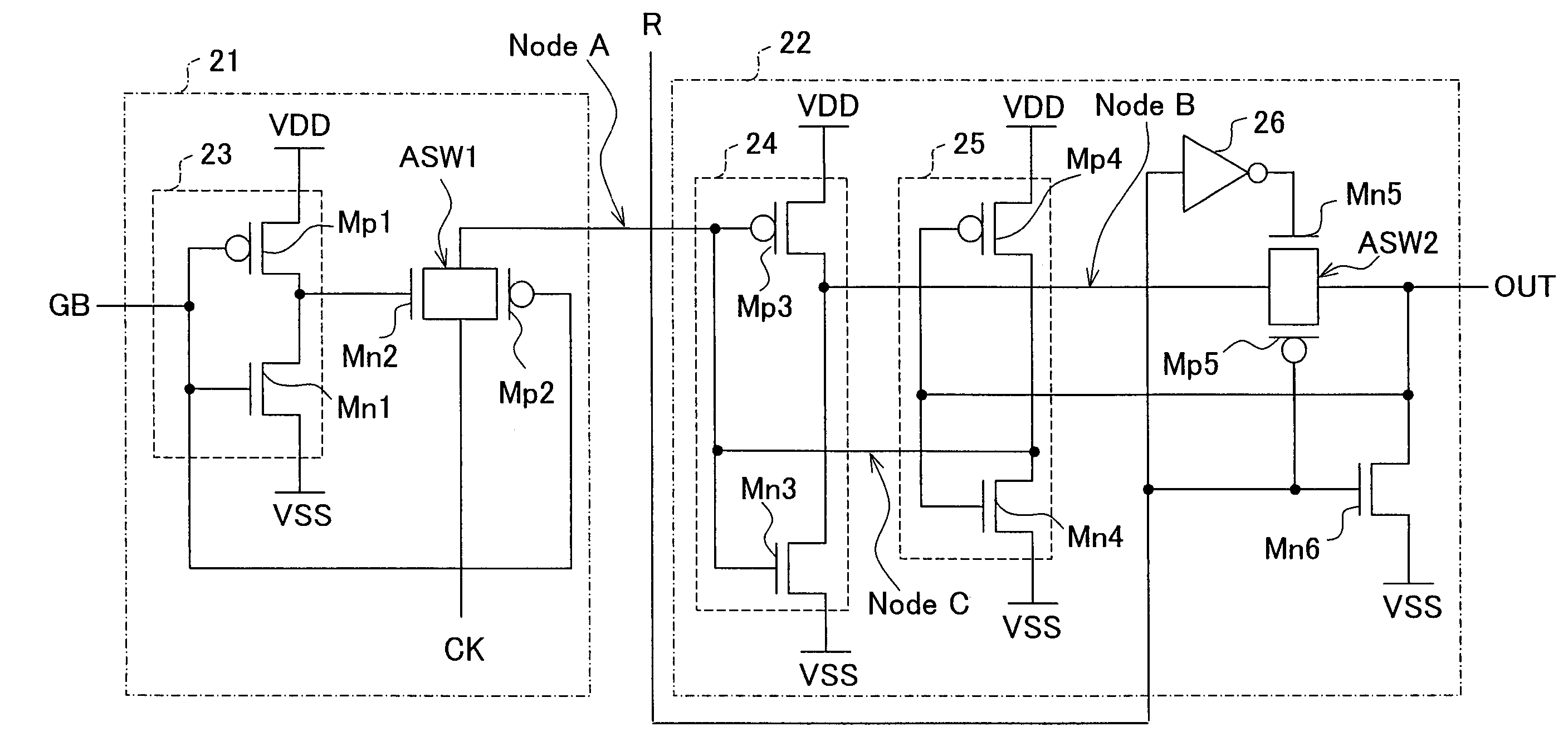
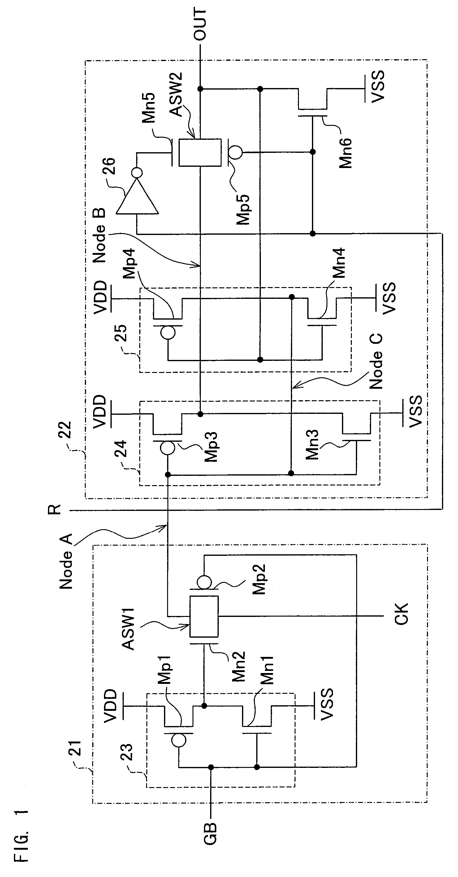
[0106]Referring to FIG. 1, the following will describe an exemplary structure of an RS flip-flop according to the First Embodiment.

[0107]The RS flip-flop shown in FIG. 1 has two major parts, a gating section 21 and a latch section 22.

[0108]The gating section 21 includes an inverter circuit 23 realized with a p-type transistor Mp1 and an n-type transistor Mn1 (hereinafter, p-type transistors and n-type transistors will be denoted by Mp and Mn, respectively), which are connected in series between power supply VDD (high potential) and VSS (low potential). A control terminal GB is connected to the input side of the inverter circuit 23, i.e., to the gates of the Mp1 and Mn1.

[0109]Between an input terminal CK and Node A is connected a CMOS analog switch ASW1 connecting Mn2 and Mp2 in parallel. In the analog switch ASW1, the gate of the Mn2 is connected to the output of the inverter circuit 23 (i.e., the junction connecting the source of Mp1 and the drain of Mn1), and the gate of Mp2 is co...

second embodiment

[0136]Referring to FIG. 5, the following will describe an exemplary structure of an RS flip-flop according to another embodiment of the invention.

[0137]The RS flip-flop shown in FIG. 5 includes two major parts, a gating section 21 and a latch section 27. As to a structure and operations of the gating section 21, no further explanation will be made because they are essentially the same as those in the RS flip-flop of the First Embodiment described with reference to FIG. 1.

[0138]The latch section 27 is similar to the latch 22 but includes an analog switch ASW3 instead of the analog switch ASW2. It is to be noted that elements of the latch section 27 having similar structures as those of the latch section 22 are given the same reference symbols and further explanations thereof will be omitted.

[0139]The analog switch ASW3 is connected between the output of the inverter 24 and the output terminal OUT of the RS flip-flop, and it serves as a CMOS analog switch connecting Mn7 and Mp7 in par...

third embodiment

[0155]Referring to FIG. 7, the following will describe an exemplary structure of an RS flip-flop according to yet another embodiment of the invention.

[0156]The RS flip-flop shown in FIG. 7 includes two major parts, a gating section 28 and a latch section 22. As to a structure and operations of the latch section 22, no further explanation will be made because they are essentially the same as those in the RS flip-flop of the First Embodiment described with reference to FIG. 1.

[0157]The gating section 28 is structured such that it receives a control signal GB, a clock signal CK, and an inverted clock signal CKB, wherein the clock signal CK and inverted clock signal CKB have amplitudes smaller than that produced by VDD, which is a power supply of the flip-flop.

[0158]In the gating section 28, Mp8 and Mn8 are connected in series between the power supply VDD and the input terminal CKB, and an Mn9 is connected between the input terminal CK and the Node A (output of the gating section 28). A...


PUM

PropertyMeasurementUnit
source-gate voltageaaaaaaaaaa

Abstract

A latch section includes a latch circuit. The latch circuit includes inverters and latches an input signal from a gating section. Between one of the inverters of the latch circuit and the output terminal OUT is disposed an analog switch whose ON / OFF characteristics are switched according to High / Low of a reset signal. Between the output terminal and an input for receiving a low potential as a power supply of a flip-flop is disposed a switching element whose ON / OFF characteristics are switched according to High / Low of the reset signal.

Description

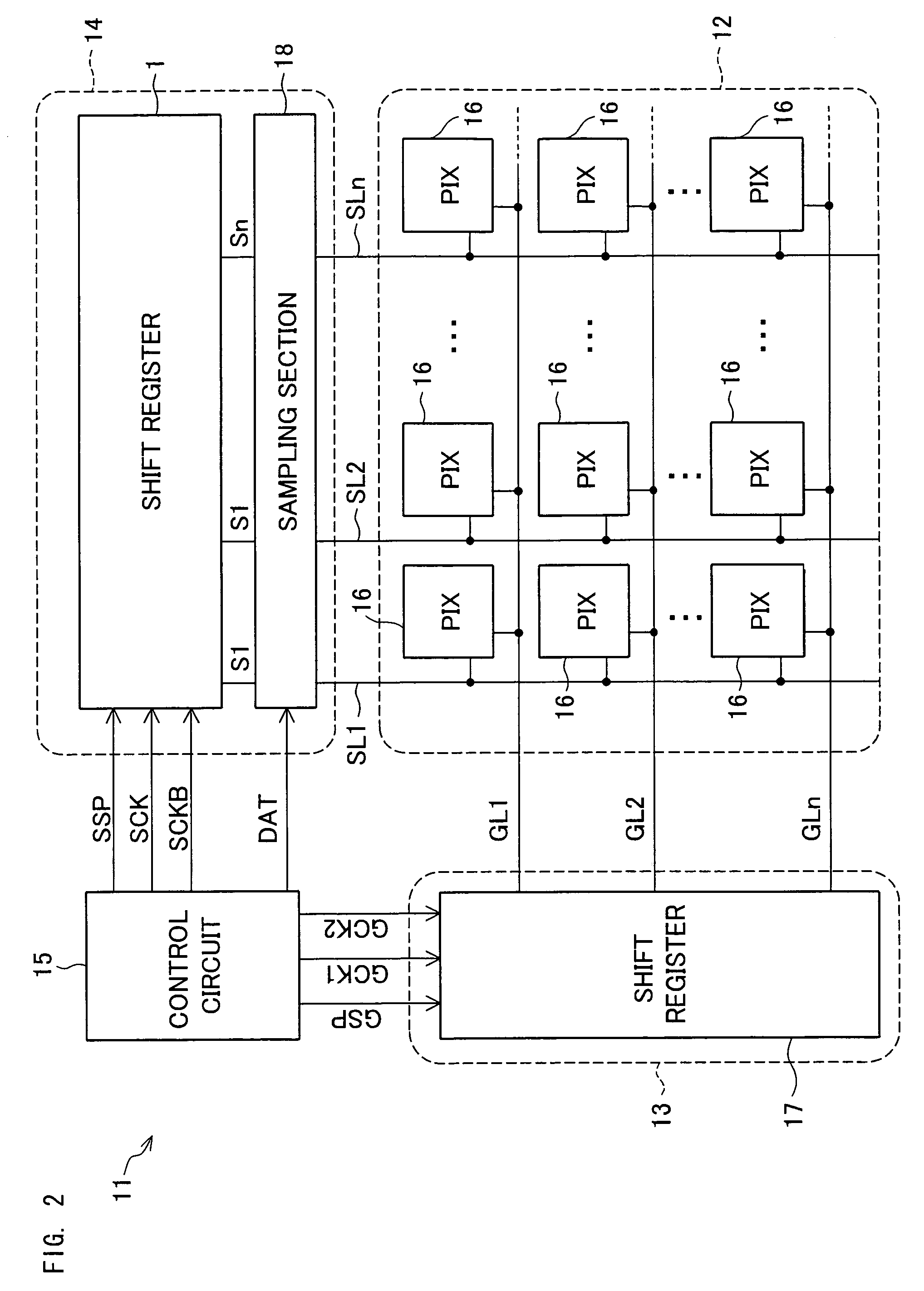
[0001]This Nonprovisional application claims priority under 35 U.S.C. § 119(a) on Patent Application No. 020342 / 2004 filed in Japan on Jan. 28, 2004, and Patent Application No. 017432 / 2005 filed in Japan on Jan. 25, 2005, the entire contents of which are hereby incorporated by reference.FIELD OF THE INVENTION[0002]The present invention generally relates to flip-flops, a shift register including multiple stages of flip-flops, and / or an active-matrix display device using the shift register for a scan signal line driving circuit or data signal line driving circuit.BACKGROUND OF THE INVENTION[0003]Active-matrix display devices require a scan signal line driving circuit and data signal line driving circuit for driving an array of pixels disposed in a matrix. The scan signal line driving circuit and data signal line driving circuit use shift registers to drive the gate lines and source lines in predetermined sequence. The shift register is realized by multiple stages of flip-flops connect...

Claims


Application Information

Patent Timeline
Patent Type & Authority Patents(United States)
IPC IPC(8): H03K3/356G02F1/133G09G3/20G09G3/30G09G3/36G11C11/412G11C19/00H03K3/012H03K3/037H03K23/00
CPCG11C19/00H03K3/356165H03K3/356113H03K3/356147H03K3/012G09G3/3677G09G3/3688B65B67/1233B65F1/1415
Inventor WASHIO, HAJIMEMURAKAMI, YUHICHIROHBROWNLOW, MICHAEL JAMES
Owner SHARP KK
Learn More