High responsivity high bandwidth metal-semiconductor-metal optoelectronic device

a metal-semiconductor and optoelectronic technology, applied in the direction of optical elements, radio frequency controlled devices, instruments, etc., can solve the problems of increasing the speed of the device, reducing the sensitivity, and general limit of the msm devi

Inactive Publication Date: 2008-09-09
RES FOUND THE CITY UNIV OF NEW YORK
View PDF11 Cites 28 Cited by
  • Summary
  • Abstract
  • Description
  • Claims
  • Application Information

AI Technical Summary

Benefits of technology

[0038]As a result, the present invention provides a high-bandwidth, high-responsivity metal-semiconductor-metal device, which is optimized for a particular operating wavelength range.

Problems solved by technology

The speed of the MSM device is generally limited by the time necessary for charges to be swept to the electrodes.
The decreased transit time results in increased speed of the device.
By reducing the spacing while maintaining a constant contact spacing, however, a large percentage of the surface of the device is covered with metallic reflective electrodes that reflect the incident light, resulting in lower sensitivity.
In other words, the MSM photodetector of the Brown patent has not been optimized for the most efficient use of SP mode coupling or any other ER mode coupling for a particular detector application.

Method used


Image

  • High responsivity high bandwidth metal-semiconductor-metal optoelectronic device
  • High responsivity high bandwidth metal-semiconductor-metal optoelectronic device
  • High responsivity high bandwidth metal-semiconductor-metal optoelectronic device

Examples


Embodiment Construction

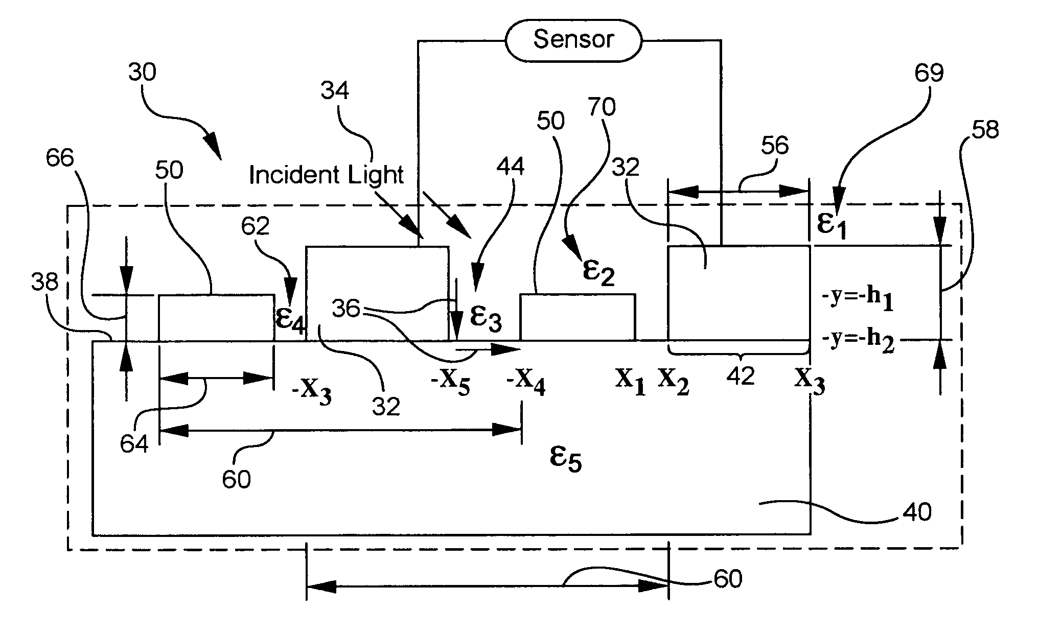
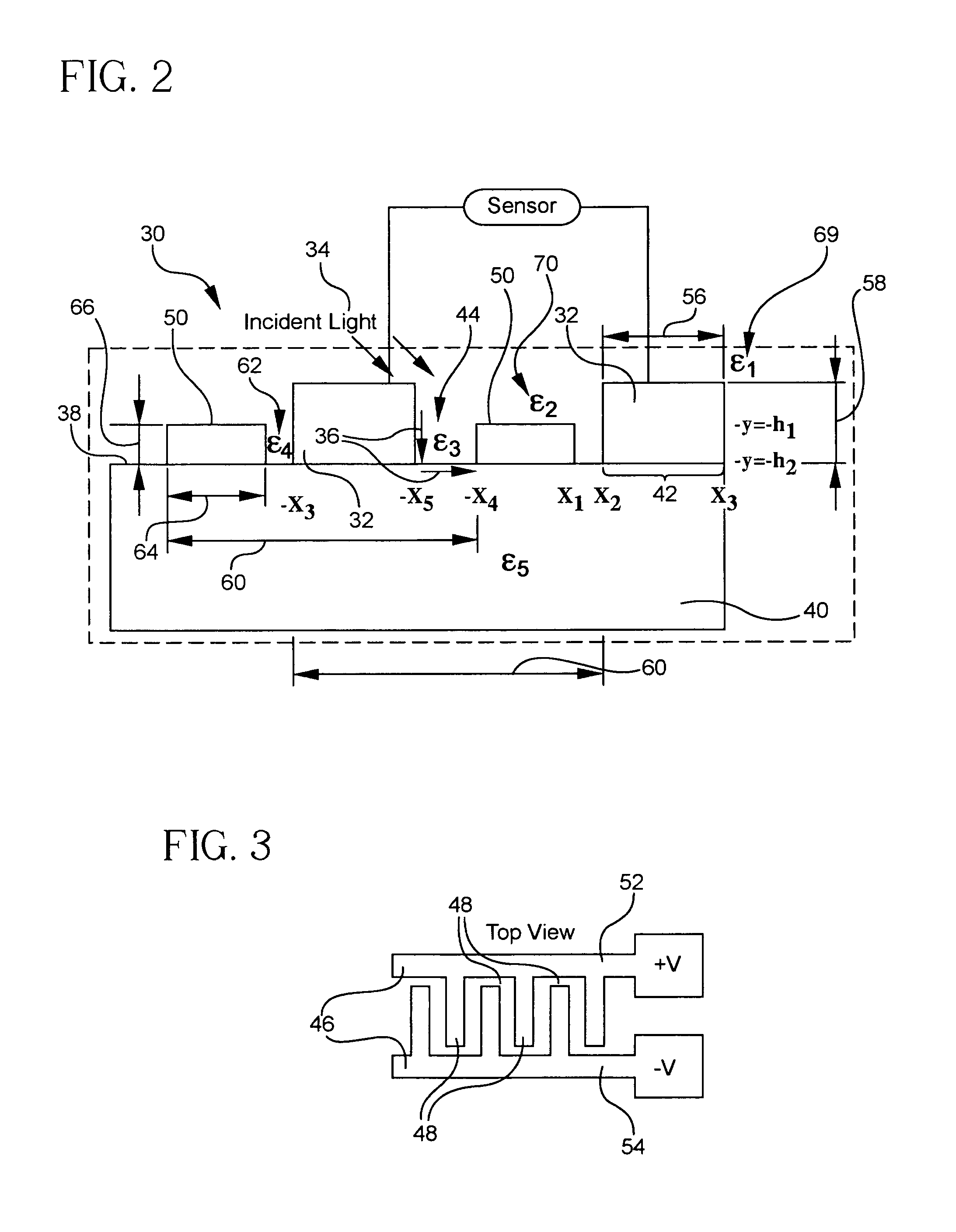
[0070]The device formed in accordance with the present invention provides an optoelectronic device with a fast response time and a high sensitivity. The structure of the device is specially tailored for optimum performance depending on the application. In particular, different applications require a sensitivity of detection within a specific wavelength range. This requirement limits the preferred semiconductor materials to those exhibiting a higher responsivity in the wavelength range of interest. Conventional devices that utilize these same semiconductors, however, do not necessarily also exhibit optimum response times, so that optoelectronic device designers must often sacrifice responsivity in exchange for higher speed.

[0071]In the present invention, the device offers high responsivity within a preferred wavelength range, while also providing high speed response times, by tailoring the structure of the electrodes to enhance both device response time and absorption of incident rad...


PUM


Abstract

An optical device for sensing an incident optical wave within a wavelength range includes a first array and a second array of electrodes superposed on a substrate, and a sensor connected to the contacts. The arrays are interdigitated. Each array includes its own parameters: contact width, contact thickness, groove width, and a groove dielectric constant. A structure associated with the arrays resonantly couples the incident wave and a local electromagnetic resonance or hybrid mode including at least a surface plasmon cavity mode (CM). For coupling the CM, an aspect ratio of contact thickness to spacing between electrodes is at least 1. A preferred structure for coupling a hybrid mode for high bandwidth and responsivity includes a higher dielectric constant in alternating grooves. The substrate may include silicon, including silicon-on-insulator (SOI). An SOI device having a alternating grooves with a higher dielectric, e.g., silicon oxide, provides 0.25 A / W and 30 GHz bandwidth.

Description

[0001]This application claims the benefit of U.S. Provisional Application No. 60 / 555,109 filed on Mar. 22, 2004, which is incorporated herein by reference.FIELD OF THE INVENTION[0002]The invention relates to the field of high responsivity optoelectronic devices and more particularly to high bandwidth, high sensitivity metal-semiconductor-metal photodetectors.BACKGROUND[0003]In prior art metal-semiconductor-metal (MSM) detectors, as light of an energy sufficiently larger than the bandgap of the semiconductor is incident on the structure, some of the incident light impinges on the semiconductor between the electrodes and excites charge carriers, i.e. electrons and holes, in the semiconductor. The electrons are swept by the applied voltage and electric field toward positively charged electrodes. The holes are swept in the opposite direction towards the negatively charged electrodes. As the charge carriers are swept to the electrodes, or contacts, they induce a measurable electrical cur...

Claims


Application Information

Patent Timeline
Patent Type & Authority Patents(United States)
IPC IPC(8): H01L31/00H01L27/12H01L31/028H01L31/0296H01L31/0304H01L31/108
CPCH01L31/1085H01L31/02327H01L31/022408H01L27/1203
Inventor AREND, MARKCROUSE, DAVID
Owner RES FOUND THE CITY UNIV OF NEW YORK
Why Eureka
Try Eureka