Power mesh for multiple frequency operation of semiconductor products

a technology of power mesh and semiconductor products, applied in the field of electronic circuit design, can solve the problems of increasing complexity of integrated circuits and chips, increasing difficulty in specifying and designing chips that perform as actually specified, and increasing the difficulty of achieving the effect of high speed and decoupling capacitan

Inactive Publication Date: 2008-09-09
AVAGO TECH INT SALES PTE LTD
View PDF6 Cites 69 Cited by
  • Summary
  • Abstract
  • Description
  • Claims
  • Application Information

AI Technical Summary

Problems solved by technology

Integrated circuits and chips have become increasingly complex and the speed and capacity of chips doubles about every eighteen months because of advances in design software, fabrication technology, semiconductor materials, and chip design.
The increased density of transistors per square centimeter and faster clock speeds, however, make it increasingly difficult to specify and design a chip that performs as actually specified.
Unanticipated and sometimes subtle interactions between the transistors and other electronic structures often adversely affect the performance of the circuit.
These difficulties increase the expense and risk of designing and fabricating chips, especially those that are custom designed for a specific application; yet the demand for complex custom-designed chips increases with the burgeoning number and variety of microprocessor-driven applications and products.
The time and money required to design chips have become a bottleneck to bring these new semiconductor products to market.
Without an assured successful outcome that the semiconductor product will be designed within a specified time and will perform as designed, the risks have risen along with costs and the result is that fewer organizations are willing to attempt the design and manufacture of custom chips.
What makes integrated circuits so expensive requiring intensive effort is that they are comprised of millions of transistors and the electrical interconnections between them.
In addition, FPGAs are very expensive and have the largest die size.
FPGAs, thus, have a high cost per function, low speed, and high power consumption.
Programmable gate arrays (PGAs) are also flexible in the number of possible applications that can be achieved but are not quite as flexible as the FPGAs and are more time-consuming to modify and test.
ASICs, however, are very complex to design and prototype because of their speed and quality.
Application Specific Standard Products (ASSPs) are hard-wired chips that meet a specific need but this customization is both time-consuming and costly.
Thus, even though the transistors may switch at higher frequencies, the collateral power grid and decoupling capacitors do not support these higher frequency functions because the increased high frequency harmonics result in increased noise.
In order to function in the realm of higher frequencies, a denser grid of power and ground lines and more decoupling capacitors are required to manage the higher power dissipation, inductance, and other electrical characteristics, but in the present technology the number of and the placement of decoupling capacitors and the power grid itself has been fixed and cannot accommodate the demand for higher performance.
Increasing the capability of the underlying grid may enable higher frequencies but reduces the density of the support transistor fabric while increases the routing difficulty.
Merely “beefing up” the grid worsens the economics of the platform.
Careful layout and review of those areas of design are also possible, allowing the frequency limits to be exceeded in small constrained areas of the design, but this approach may not work for all designs and, more importantly, it is extremely time-consuming demanding intensive engineering.
Increasing bus widths in order to limit frequency requirements is workable but that approach increases the latency for data passing through the system.
Increasing the bus size by two or more increases routing complexity by much more.
Thus, there is an inevitable compromise between high frequency and power requirements.
Processor architecture is a complete science onto itself and is as complex or more so than high speed communications which may be encompassed within the processing and data availability requirements.
Because there are so many variations in the applications, the data, the speeds, and standards, it is very expensive and burdensome to design and manufacture individual full custom chips for specific applications, specific processors, and protocols.

Method used


Image

  • Power mesh for multiple frequency operation of semiconductor products
  • Power mesh for multiple frequency operation of semiconductor products
  • Power mesh for multiple frequency operation of semiconductor products

Examples


Embodiment Construction

in conjunction with the accompanying figures.

BRIEF DESCRIPTION OF THE DRAWINGS

[0016]The numerous advantages of the present invention may be better understood by reference to the accompanying figures in which:

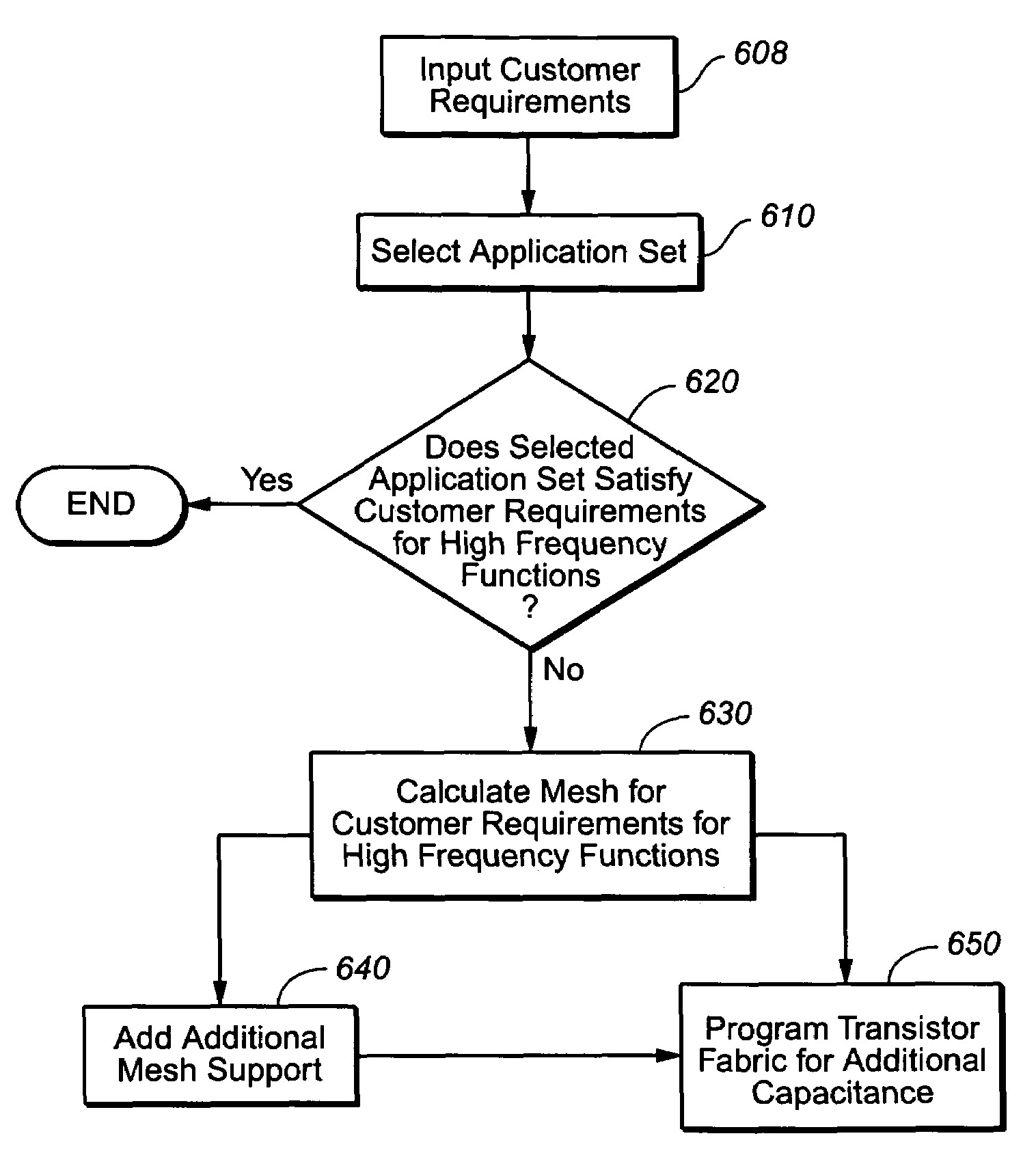
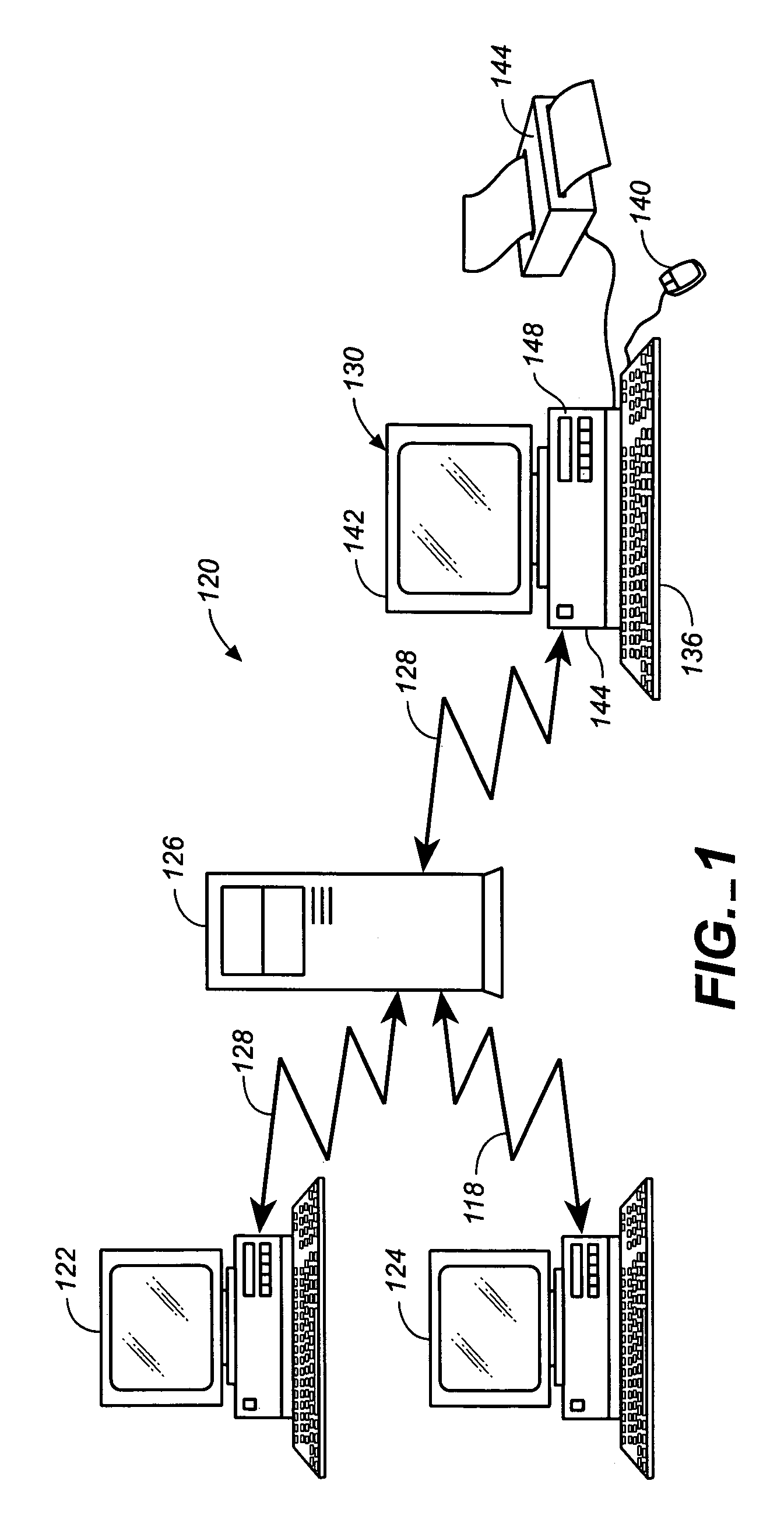
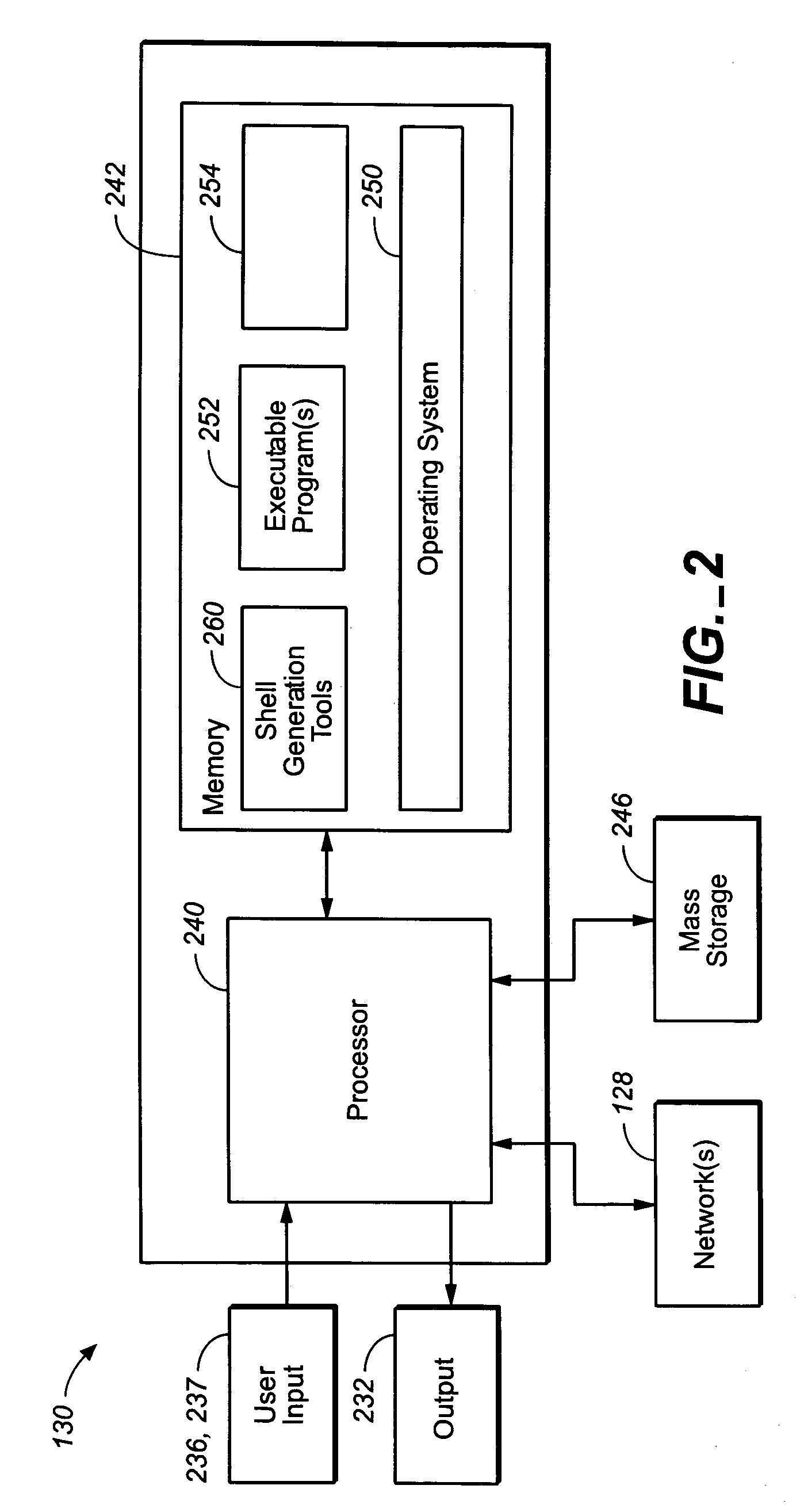
[0017]FIGS. 1 and 2 are simplified block diagrams of a computer network and a computer processor implementing the method by which a semiconductor platform having the multiple frequency grid of the invention can be fabricated in accordance with an embodiment of the invention.

[0018]FIG. 3 is a simplified block diagram of a semiconductor product that is an example of one that can take advantage of an implementation the multiple frequency grid of the invention.

[0019]FIG. 4 is a simplified block diagram of the semiconductor product as above but having an application set upon which the multiple frequency power mesh of the invention has been fabricated in accordance with an embodiment of the invention.

[0020]FIGS. 5a, 5b, and 5c are different embodiments of a localized grid that can be ...


PUM


Abstract

The design of integrated circuits, i.e., semiconductor products, is made easier with a semiconductor platform having versatile power mesh that is capable of supporting simultaneous operations having different frequencies on the semiconductor product; e.g., higher frequency operations may be embedded as diffused blocks within the lower layers or may be programmed from a configurable transistor fabric above the diffused layers. Preferably the power mesh is located above the layers having the operations requiring the different frequencies, and may be fixed in an application set given to a chip designer or may be configurable by the designer her / himself. For example, to support high speed communications adjacent an embedded high speed data transceiver, the transistor fabric may be programmed as a data link layer having higher performance requirements than the rest of the integrated circuit. The data link layer may be connected to one of the localized grids of the versatile power mesh which may have an increased density and / or wider strap width of a power / ground grid. Additional decoupling capacitance can be embedded in the lower layers of the semiconductor product and / or can be programmed from the configurable transistors fabric.

Description

FIELD OF THE INVENTION[0001]This invention relates generally to the field of electronic circuit design and more particularly relates to a semiconductor platform having a configurable power mesh for multiple frequency and power requirements on a semiconductor product.BACKGROUND[0002]Integrated circuits and chips have become increasingly complex and the speed and capacity of chips doubles about every eighteen months because of advances in design software, fabrication technology, semiconductor materials, and chip design. The increased density of transistors per square centimeter and faster clock speeds, however, make it increasingly difficult to specify and design a chip that performs as actually specified. Unanticipated and sometimes subtle interactions between the transistors and other electronic structures often adversely affect the performance of the circuit. These difficulties increase the expense and risk of designing and fabricating chips, especially those that are custom design...

Claims


Application Information

Patent Timeline
Patent Type & Authority Patents(United States)
IPC IPC(8): G06F17/50
CPCG06F17/5045G06F30/30
Inventor VOGEL, DANNY CARLDEISZ, DANIEL
Owner AVAGO TECH INT SALES PTE LTD
Why Eureka
Try Eureka