Lithographically optimized placement tool

a placement tool and lithographic optimization technology, applied in the field of integrated circuit design, can solve the problems of affecting the functionality of the circuit, affecting the layout of the circuit, and catastrophic yield loss, and achieve the effect of improving the performance of the circui

Active Publication Date: 2008-10-07
SYNOPSYS INC
View PDF4 Cites 4 Cited by
  • Summary
  • Abstract
  • Description
  • Claims
  • Application Information

AI Technical Summary

Benefits of technology

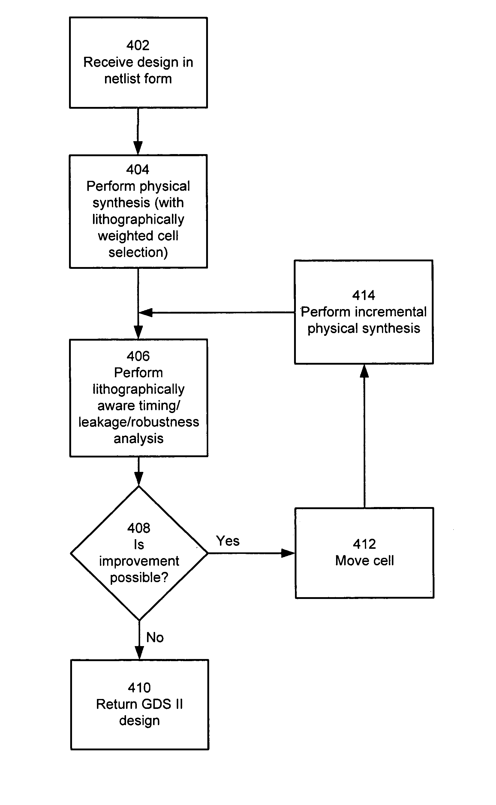
[0010]One embodiment of a disclosed method (and system) includes analyzing the results of a lithographic simulation and moving circuit elements to improve the performance of the circuit under lithographic variation.

Problems solved by technology

When not properly accounted for, these optical effects can cause differences between the circuit layout and the circuit as fabricated.
These differences can potentially affect the functionality of the circuit, such as the leakage current and timing performance.
In certain circumstances, these optical effects can result in catastrophic yield loss.
In practice, the conditions used to fabricate a circuit will rarely match these optimal conditions exactly.
Variation in the lithographic process (“lithographic variation”), such as variation in the exposure and in the focus of the lithographic process, tends to reduce the effectiveness of optical proximity correction.
Even with optical proximity correction, certain fabrication conditions can potentially affect the functionality of the fabricated circuit.
However, restrictive design rules significantly limit the place and route tool, and applying generalized rules often results in sub-optimal designs, as the rules are followed even in circumstances when they are not strictly necessary.
While restrictive design rules improve the probability of successful lithographic fabrication, they are often overly restrictive and result in a significant increase in the area occupied by a circuit.
As reducing circuit size is a goal of most integrated circuit design, the increase in circuit size caused by restrictive design rules is usually an undesirable result.

Method used


Image

  • Lithographically optimized placement tool
  • Lithographically optimized placement tool
  • Lithographically optimized placement tool

Examples


Embodiment Construction

[0024]As used herein, the terms “comprises,”“comprising,”“includes,”“including,”“has,”“having” or any other variation thereof, are intended to cover a non-exclusive inclusion. For example, a process, method, article, or apparatus that comprises a list of elements is not necessarily limited to only those elements but may include other elements not expressly listed or inherent to such process, method, article, or apparatus. Further, unless expressly stated to the contrary, “or” refers to an inclusive or and not to an exclusive or. For example, a condition A or B is satisfied by any one of the following: A is true (or present) and B is false (or not present), A is false (or not present) and B is true (or present), and both A and B are true (or present).

[0025]Also, use of the “a” or “an” are employed to describe elements and components of the invention. This is done merely for convenience and to give a general sense of the invention. This description should be read to include one or at ...


PUM


Abstract

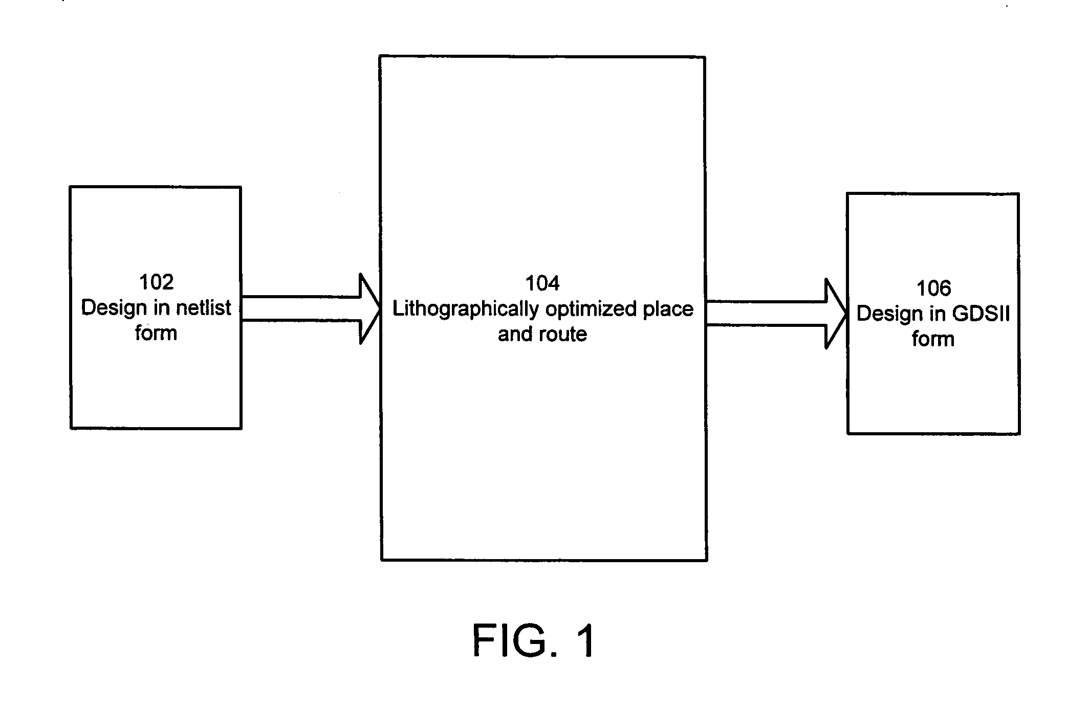
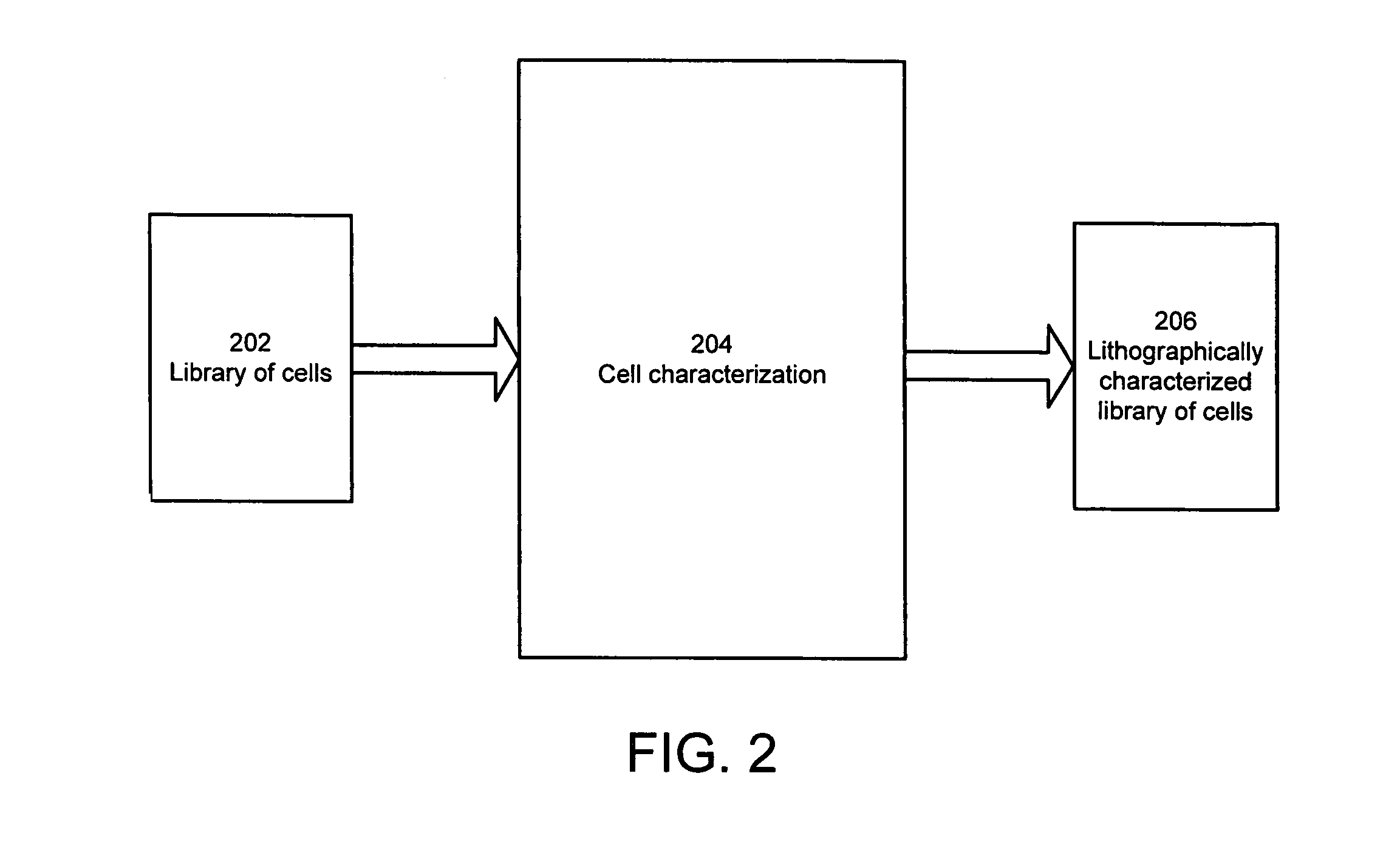
A system and a method are disclosed for integrating the results of lithographic simulation into the physical synthesis process. The effects of lithographic variation are considered when selecting a cell from among a group of cells having equivalent function. Circuit design elements are placed and routed with consideration of the effects of lithographic variation on robustness, timing performance, and leakage current. Cells may be simulated under a variety of conditions and environments and the simulation results stored in a library for efficient lithographically optimized placements.

Description

BACKGROUND[0001]1. Field of the Art[0002]The present invention generally relates to the field of integrated circuit design, and more specifically, to the placement and routing of the elements of an integrated circuit design.[0003]2. Description of the Related Art[0004]In integrated circuit fabrication, lithographic techniques are often employed to create circuit features. In order to satisfy demand for smaller circuits consuming less power, fabrication techniques are continually pushed in the direction of producing smaller and smaller features. Existing lithographic technology is capable of creating circuit features of size of similar magnitude to that of the wavelength of light used to create the features themselves. As circuit features become smaller, common optical effects such as diffusion, diffraction, and dispersion begin to significantly influence the results achieved by the fabrication. When not properly accounted for, these optical effects can cause differences between the ...

Claims


Application Information

Patent Timeline
Patent Type & Authority Patents(United States)
IPC IPC(8): G06F17/50
CPCG06F17/5072G06F30/392
Inventor DEVGAN, ANIRUDHMETCALFE, RODERICKRAGHAVAN, VIVEKWONG, ALFRED
Owner SYNOPSYS INC
Why Eureka
Try Eureka