Exposure system, exposure method and method for manufacturing a semiconductor device

a semiconductor and exposure system technology, applied in the field of semiconductor device manufacturing technology, can solve the problems of increasing the dimensional variation of the resist pattern, difficult to form fine resist patterns, and inability to obtain sufficient process windows in some cases

Inactive Publication Date: 2008-10-14
KK TOSHIBA
View PDF12 Cites 16 Cited by
  • Summary
  • Abstract
  • Description
  • Claims
  • Application Information

AI Technical Summary

Problems solved by technology

Such a fine resist pattern is difficult to form even using the normal or annular illumination.
However, the patterns are increasingly miniaturized, and in the case of forming a fine resist pattern such as a row of hole patterns having a cycle length not more than three quarter wavelength, a sufficient process window cannot be obtained in some cases, even using the tripole illumination.
Thus, there is a problem of increasing dimensional variation in the resist pattern.

Method used


Image

  • Exposure system, exposure method and method for manufacturing a semiconductor device
  • Exposure system, exposure method and method for manufacturing a semiconductor device
  • Exposure system, exposure method and method for manufacturing a semiconductor device

Examples


first modification

(First Modification)

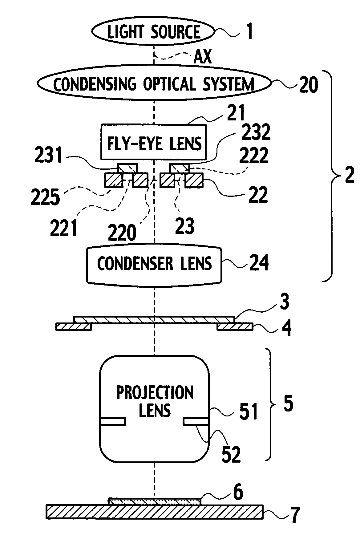
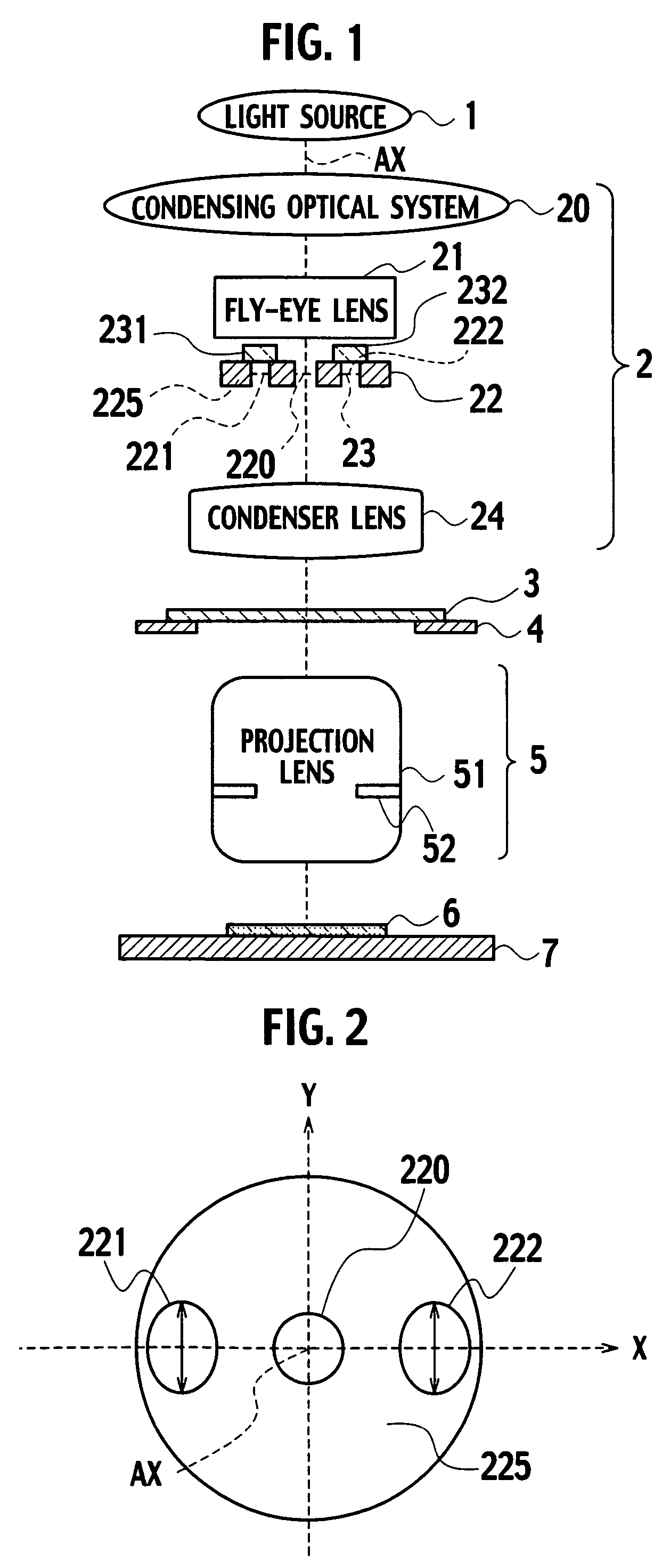
[0082]In a first modification of the embodiment of the present invention, the vibration direction of the electric vectors of the light emitted from the light source 1, shown in FIG. 1, is extended in the perpendicular direction (Y-axis direction) to the straight line passing through the first and second eccentric regions 221 and 222, shown in FIG. 2. As shown in FIG. 15, a quarter wave plate 250 is placed in the optical path of the light passing through the center region 220 of the effective illumination source plane 23 in a plane conjugate with the effective illumination source plane 23. The quarter wave plate 250 changes the incident linearly polarized light into circularly polarized light. As shown in FIG. 2, therefore, in the effective illumination source plane 23, obliquely incident light which is linearly polarized such that the vibration direction of the electric vectors is extended in the isolation direction of the mask pattern 31 are formed by each of th...

second modification

(Second Modification)

[0086]In a second modification of the embodiment of the present invention, a description is given of an example, in which, as shown in FIG. 18, the vibration directions of the electric vectors of the perpendicularly incident light passing through the center region 220 is equal to the parallel direction (X-axis direction) to the straight line connecting the first and second eccentric regions 221 and 222. As shown in FIG. 19, a half wave plate 260 is placed in the optical path passing through the center region 220 of the effective illumination source plane 23 in a plane conjugate with the effective illumination source plane 23. The half wave plate 260 rotates the vibration directions of the electric vectors of incident linear polarized light by 90 degrees.

[0087]In the effective illumination source plane 23, as shown in FIG. 18, the perpendicularly incident light passing through the center region 220 is linearly polarized. The vibration direction of the electric ve...

third modification

(Third Modification)

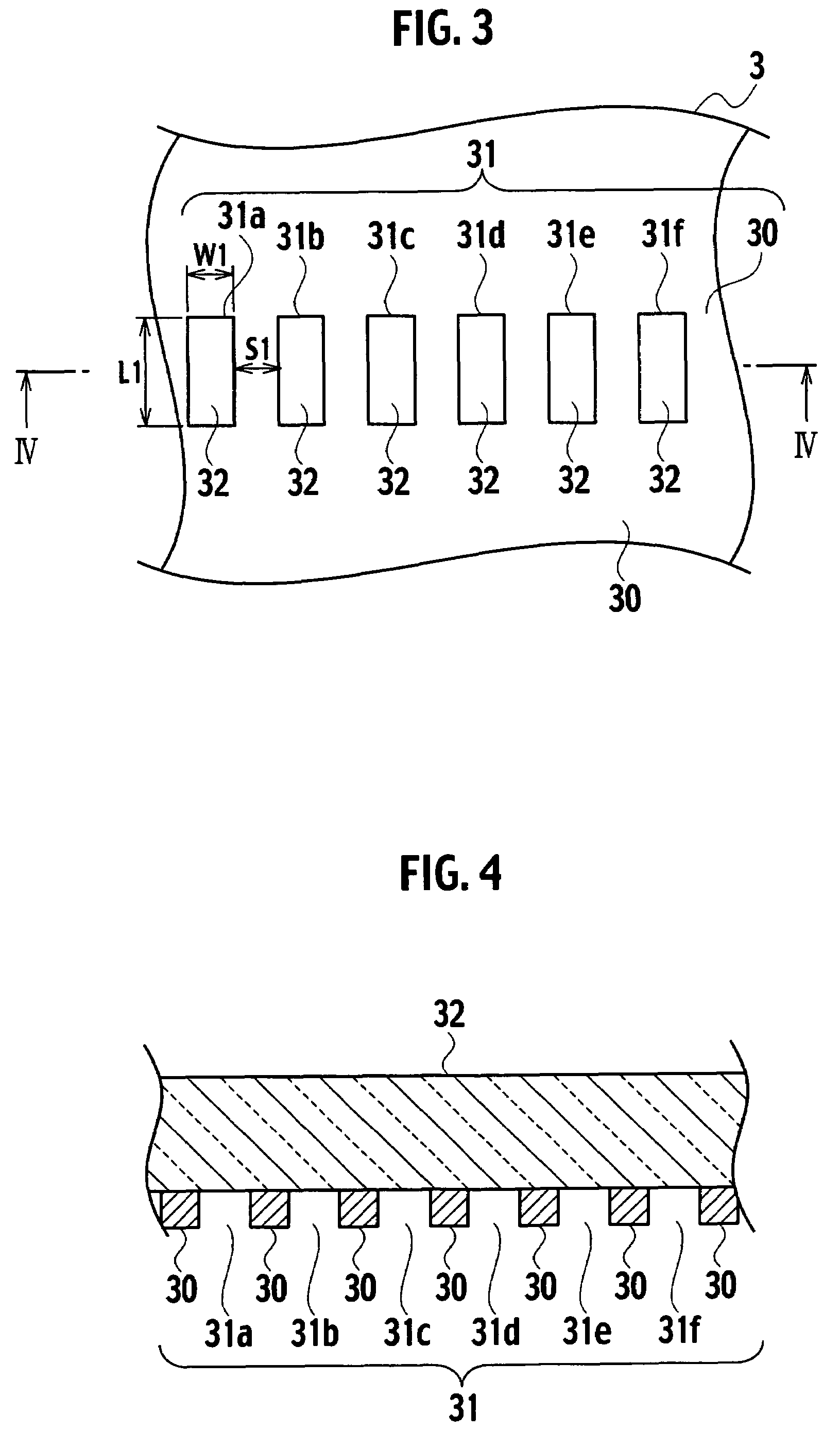
[0091]In a third modification of the embodiment of the present invention, as shown in FIG. 21, a description is given of an example in which the photoresist 3 includes patterns 331, 332, and 333 of various shapes in addition to the mask pattern 31 with the openings 31a to 31f. The pattern 331 shown in FIG. 21 is a thin line pattern extending in the isolation direction of the openings 31a to 31f. The pattern 332 is a rectangular pattern. The pattern 333 is a thin line pattern extending in the cyclic direction of the openings 31a to 31f.

[0092]In the projection exposure using the photomask 3 shown in FIG. 21, using the tripole illumination shown in FIGS. 2 and 18, the exposure latitude with respect to the dimension in the isolation direction is different from the exposure latitude with respect to the dimension in the cyclic direction, resulting in problems. This is because the illumination is different between the isolation direction of the openings 31a to 31f and ...


PUM

PropertyMeasurementUnit
wavelengthaaaaaaaaaa

Abstract

An exposure system includes: an illumination optical system defining, in an effective illumination source plane, a center region forming a perpendicularly incident light and first and second eccentric regions forming obliquely incident lights having a perpendicular electric vector component perpendicular to a straight line connecting the first and second eccentric regions, the electric vector component being larger than a parallel electric vector component parallel to the straight line, and illuminating the mask pattern with the perpendicularly incident light and the obliquely incident lights; and a projection optical system projecting an image of the mask pattern to a processing object.

Description

CROSS REFERENCE TO RELATED APPLICATIONS AND INCORPORATED BY REFERRENCE[0001]The application is based upon and claims the benefit of priority from the prior Japanese Patent Applications No. P2004-368098, filed on Dec. 20, 2004; the entire contents of which are incorporated herein by reference.BACKGROUND OF THE INVENTION[0002]1. Field of the Invention[0003]The present invention relates to technology for manufacturing a semiconductor device, more particularly, to an exposure system, an exposure method and a method for manufacturing a semiconductor device.[0004]2. Description of the Related Art[0005]In a photolithography process for manufacturing a semiconductor device, illumination light emitted from an effective illumination source (secondary illumination source) formed in an illumination optical system illuminates a mask pattern provided on a photomask (reticle). The illumination light diffracted at the photomask is concentrated on a resist film applied on a semiconductor substrate b...

Claims


Application Information

Patent Timeline
Patent Type & Authority Patents(United States)
IPC IPC(8): G03B27/72G03B27/42G03B27/54G03F7/20G03F7/40
CPCG03F7/70091G03F7/701G03F7/70125G03F7/70566
Inventor FUKUHARA, KAZUYA
Owner KK TOSHIBA
Why Eureka
Try Eureka