Pulse generating circuit, electronic device using this pulse generating circuit, cellular phone set, personal computer, and information transmitting method using this circuit

a technology of pulse generating circuit and pulse generating circuit, which is applied in the direction of pulse technique, generating/distributing signals, instruments, etc., can solve the problems of increasing power consumption, difficult or impossible to obtain such an element, and heavy use of waveform shown here, so as to facilitate wireless transmission of the required information and reduce power consumption. the effect of significant

Active Publication Date: 2008-11-11
138 EAST LCD ADVANCEMENTS LTD
View PDF4 Cites 14 Cited by
  • Summary
  • Abstract
  • Description
  • Claims
  • Application Information

AI Technical Summary

Benefits of technology

[0012]Accordingly, an advantage of some aspects of the invention is to provide a pulse generating circuit that is capable of easily generating a high-frequency band pulse, simple in structure and that consumes little power, an electronic device using this circuit, and a method of transmitting information using this circuit.

Problems solved by technology

However, the waveform shown here is in heavy usage since the method of generation it is easy.
However, in fact, it is very difficult or impossible to obtain such an element.
Generally, when an attempt is made to operate the element at a high speed, an increase in power consumption results.
Therefore, when an attempt is made to obtain a very short pulse in such a circuit, an increase in power consumption is inevitable in the related art.

Method used


Image

  • Pulse generating circuit, electronic device using this pulse generating circuit, cellular phone set, personal computer, and information transmitting method using this circuit
  • Pulse generating circuit, electronic device using this pulse generating circuit, cellular phone set, personal computer, and information transmitting method using this circuit
  • Pulse generating circuit, electronic device using this pulse generating circuit, cellular phone set, personal computer, and information transmitting method using this circuit

Examples


first embodiment

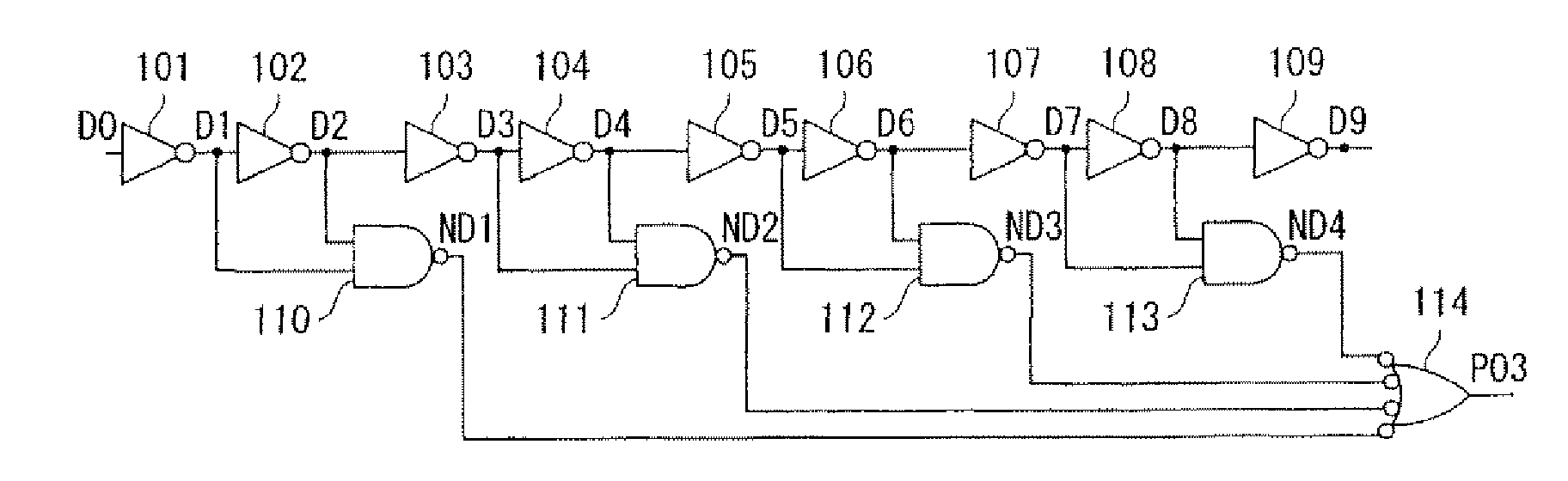
[0081]FIG. 1A is a circuit diagram showing a principal portion of a pulse generating circuit according to a first embodiment of the invention, FIGS. 1B to 1D are time charts for describing the operation thereof. However, the description will be made of an example in which the pulse waveform assumes a shape as shown in FIG. 6A and four pulses are contained in a time PD (PD=8Pw) that is, a pulse whose number of fingers is four.

[0082]Reference numerals 101 to 109 shown in FIG. 1A are cascaded inverter circuits. The respective input / output terminals are designated by terminal names such as D-0 to D9.

[0083]When the input terminal D0 is changed from a high level (H) to a low level (L) as shown in FIG. 1B, the respective outputs are propagated with the delay of t. NOT-AND (NAND) circuits 110 to 113 output L from the terminals ND1 to ND4 as shown in FIG. 1C when both D1 and D2, D3 and D4, D5 and D6, and D7 and D0 are H, respectively. The NEITHER-NOR (NOR) circuit (NOR circuit of negative lo...

second embodiment

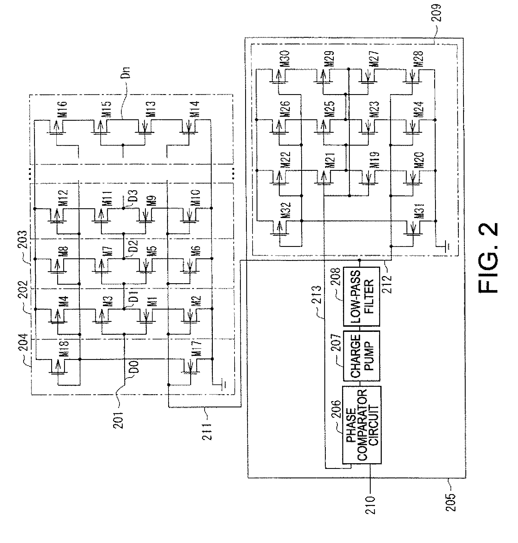
[0089]FIG. 2 is a circuit diagram showing a principal portion of a pulse generating circuit according to a second embodiment of the invention.

[0090]Reference numerals 202, 203 designate inverter circuits in which the amount of delay can be controlled and correspond to the inverter circuits 101, 102 which constitutes the delay circuit in the first embodiment. The equivalent circuits are arranged in the required number of stages for use. In FIG. 2, those from the third stage on are not numbered. The inverter circuit 202 is configured by a combination of a PMOS transistor M3 and an NMOS transistor M1.

[0091]PMOS and NMOS transistors M4 and M2 are connected to sources of the respective transistors M3 and M1, and the amount of delay can be controlled by controlling the amount of electric current flowing into the inverter circuit by the M4 and M2.

[0092]A gate of the transistor M2 is connected to a control voltage terminal 211, and a gate of the transistor M4 is connected to the control vol...

third embodiment

[0103]FIG. 3 is a circuit diagram showing a principal portion of a pulse generating circuit according to a third embodiment of the invention.

[0104]Reference numerals 311 to 314 are buffer circuits configured of current mode logic circuits. The contents thereof will be described with the buffer circuit 311 as an example. A differential amplifier circuit is configured by an NMOS transistor differential pair M1 and M2. The NMOS transistor M3 controls the amount of delay by controlling the circuit current according to a control voltage 310 applied to the gate. PMOS transistors M4, M5 are loads on the output side and control the output amplitude by the gate application voltage. Input and output of the buffer circuit 311 is driven by a differential signal which is a characteristic of the current mode logic circuit.

[0105]The terminal 301 is a trigger terminal which corresponds to the terminal D0 in the first embodiment, and intended pulses are generated on the basis of the pulses which are...


PUM


Abstract

A pulse generating circuit includes a plurality of delay elements cascaded so as to constitute a predetermined loop, wherein when a predetermined input pulse is supplied to a leading end of the series connection, an effective frequency multiplication is applied to signals which appear at a plurality of portions out of the node portions among the plurality of delay elements and the terminal end portion of the series connection by a logical circuit to obtain an output pulse having a higher frequency than the input pulse.

Description

BACKGROUND[0001]1. Technical Field[0002]The present invention relates to a pulse generating circuit, suitable for an UWB (Ultra Wide Band), an electronic device using this circuit, and a method of transmitting information using this circuit.[0003]2. Related Art[0004]UWB communication is a communication system for performing high-speed and high-capacity data communication using a very wide frequency band. A communication system using a wideband signal includes a method using a spread spectrum and a method of orthogonal frequency division multiplex (OFDM) in the related art. However, UWB is a communication system of a wider band using very short pulses, and is also referred to as a communication of an impulse radio (IR) system. In the IR system, modulation and demodulation are possible only by operating a time axis which does not depend on modulation in the related art, and it is considered that simplification of the circuit or reduction of power consumption can be expected (see U.S. ...

Claims


Application Information

Patent Timeline
Patent Type & Authority Patents(United States)
IPC IPC(8): G06F1/04
CPCH03K3/0315H03K5/00006H03K5/133H03L7/0805H03L7/0995H04B1/7174H03K2005/00039
Inventor IKEDA, MASAYUKI
Owner 138 EAST LCD ADVANCEMENTS LTD
Why Eureka
Try Eureka