Optical waveguide device and optical modulator

a technology of optical modulator and optical waveguide, which is applied in the direction of optical waveguide light guide, instruments, optics, etc., can solve the problems of loss degradation, enlargement of the entire optical modulator, deterioration of the polarization-extinction ratio of output signals, etc., and achieves simple optical waveguide structure and high polarization-extinction ratio

Inactive Publication Date: 2008-11-11
FUJITSU LTD
View PDF2 Cites 17 Cited by
  • Summary
  • Abstract
  • Description
  • Claims
  • Application Information

AI Technical Summary

Benefits of technology

[0019]The present invention has been accomplished in view of the above problems, and has an object to provide an optical waveguide device having a simple optical waveguide structure capable of selectively attenuating one of orthogonal polarization modes of a light propagated through an optical waveguide. Further, the present invention has an object to provide an optical modulator which is applied with the above optical waveguide structure, to thereby realize a high polarization-extinction ratio.
[0022]An optical modulator according to the present invention comprises: a substrate having an electro-optic effect; an optical waveguide comprising a core which is formed on the substrate and has the relatively high refractive index, and a cladding which is arranged so as to cover the core and has the relatively low refractive index; an electrode arranged in the vicinity of the optical waveguide; and a buffer layer which is arranged between the optical waveguide and the electrode to suppress the optical absorption by the electrode, for modulating a light being propagated through the optical waveguide due to the electro-optic effect caused by a drive voltage applied on the electrode, wherein the buffer layer has a multi-layer structure in which one or more low refractive index layers formed using a material of the refractive index lower than that of the core and one or more high refractive index layers formed using a material of the refractive index higher than that of the core are laminated in a direction toward the electrode from the core, and a lamination cycle of the low refractive index layer and the high refractive index layer in the multi-layer structure is set to be shorter than a distance to which a polarization mode for guiding the core leaks out to a single-layer buffer on the assumption that the single-layer buffer is formed using the material constituting the low refractive index layer. In the optical modulator having such a configuration, since the buffer layer between the optical waveguide and the electrode is made to have the multi-layer structure by the lamination of the low refractive index layers and the high refractive index layers, the optical waveguide of large polarization dependence is realized due to the structural birefringence of the buffer layer of the multi-layer structure, and the improvement of polarization-extinction ratio is achieved.
[0023]As described in the above, according to the optical waveguide device of the present invention, it is possible to increase the polarization dependence of the leakage of the light being propagated through the optical waveguide out to the cladding, by utilizing the structural birefringence of the multi-layer structure portion of the cladding. Therefore, it becomes possible to, without increasing the loss to the one polarization mode of the propagated light, selectively attenuate the other polarization mode.
[0024]By making the buffer layer between the optical waveguide and the electrode to have the multi-layer structure by applying the above optical waveguide structure to the optical modulator, since the structure itself of the optical modulator is provided with a function as a polarizer, it becomes possible to improve a polarization-extinction ratio of a modulated signal. Further, the above optical modulator can be produced utilizing the process similar to the conventional process, and also there is no need to extend the chip length. Therefore, there is no possibility of an excess loss in the guided mode or an increase of drive voltage.

Problems solved by technology

However, it is impossible to avoid that the polarized wave (the TM mode in the x-cut substrate, and the TM mode in the z-cut substrate) orthogonal to the z-axis direction is incident or excited, due to the axis deviation between a modulator chip and an input fiber, the polarization variation of the incident light, the lack of polarization-extinction ratio in the waveguide itself or the like, resulting in the deterioration in polarization-extinction ratio of an output signal.
However, the following problems are caused, considering the integration or the unification of each polarizer with an optical waveguide device, such as the optical modulator or the like as described above.
Firstly, with regard to the waveguide type polarizer by the method of (1) or (2), as shown in an upper stage of FIG. 30 for example, since it is required to dispose a polarizer portion of a few millimeters to a few centimeters on an incident port side (or an emission port side) of the optical modulator or the like, the chip length is increased, resulting in the size enlargement of the entire optical modulator or in the loss degradation thereof.
In the case where the waveguide type polarizer by the method of (1) or (2) is used, to thereby realize the improvement of the polarization-extinction ratio of the optical waveguide device, such as the optical modulator or the like, there is a problem in that the various characteristics (for example, the chip length, an insertion loss, the drive voltage and the like) of the conventional optical waveguide device are degraded.
However, considering the LN optical modulator for example, in an actual situation, there has not been known a material indicating the appropriate birefringence in the vicinity of the refractive index of LiNbO3.
Even if such a material is obtained, it is necessary to match an orientation of the birefringent material to be used for the cladding with the crystal direction of the LiNbO3 substrate with high precision, and therefore, there is a problem in that such a waveguide is hard to be practically produced.
However, there is a drawback in that the producing process becomes complicated, resulting in the cost increase.
With regard to the waveguide type polarizer by the method of (4), there is a problem in that the drive voltage (Vπ) is relatively high in the optical modulator to which the proton-exchange waveguide is applied.
With regard to the waveguide type polarizer by the method of (5), the structure of the waveguide is complicated, and a leakage amount (polarization-extinction ratio) of one of the polarization mode lights greatly depends on the film thickness of the cladding.
Therefore, the film thickness control is significantly difficult, causing a problem in the producing performance.

Method used


Image

  • Optical waveguide device and optical modulator
  • Optical waveguide device and optical modulator
  • Optical waveguide device and optical modulator

Examples


first embodiment

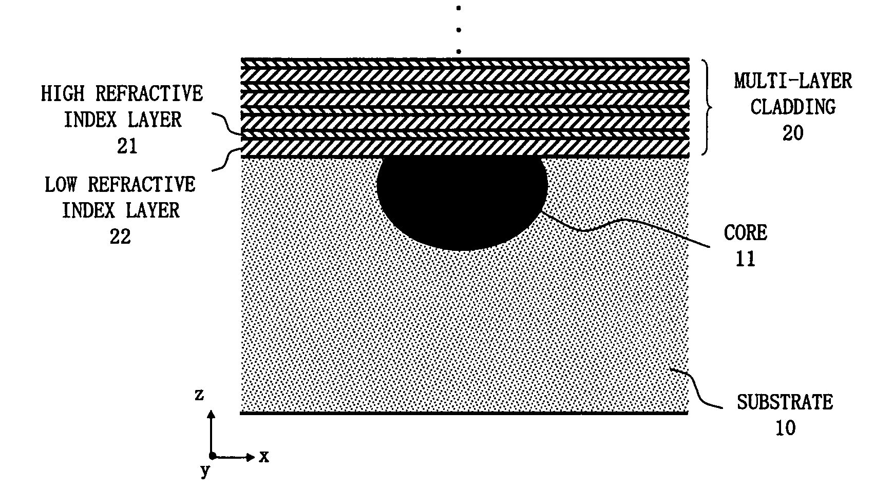
[0102]FIG. 20 is a cross section view showing a configuration of the optical waveguide device according to the present invention.

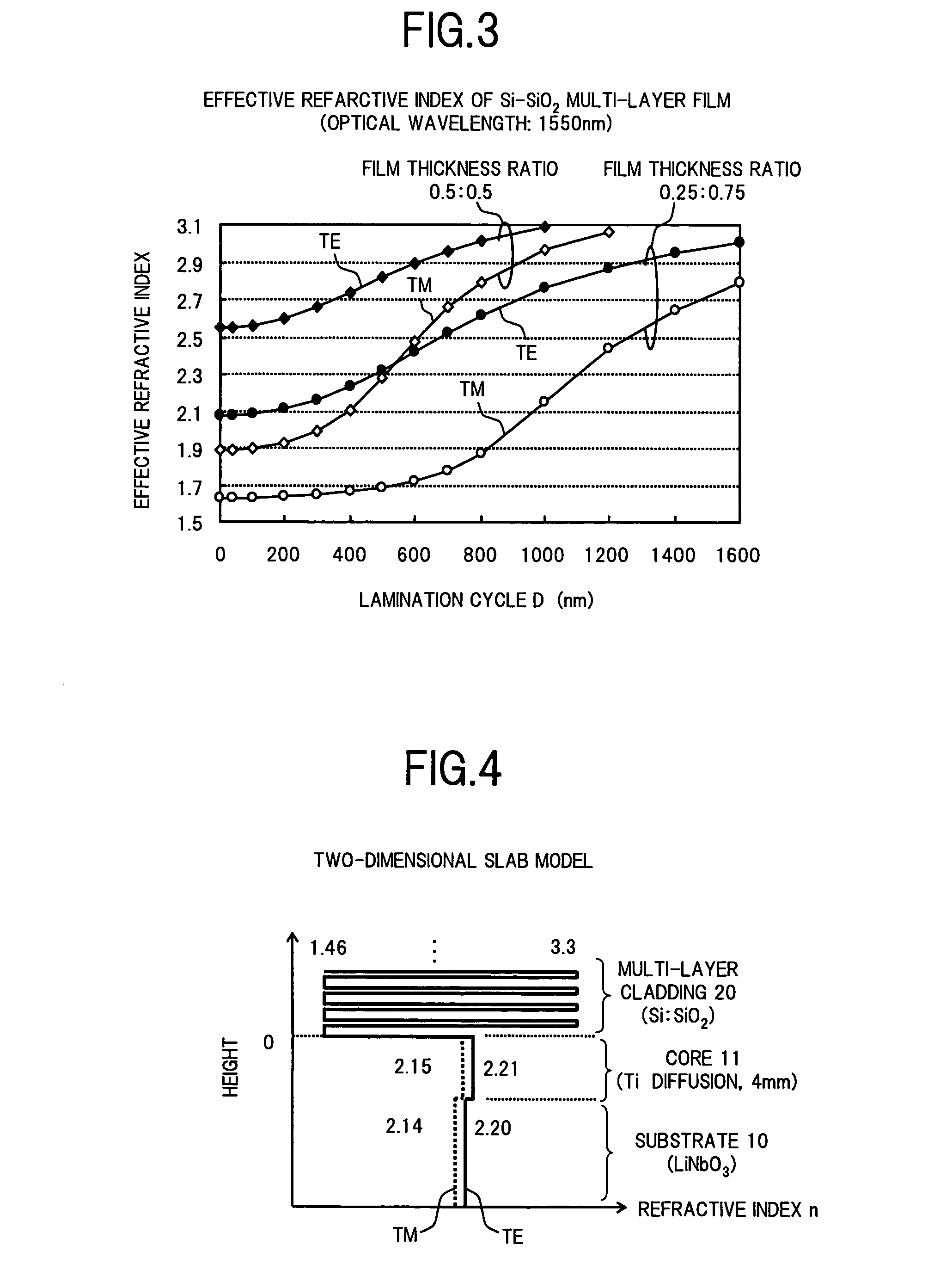
[0103]In the first embodiment, a waveguide type polarizer is realized such that the core 11 is formed on the LiNbO3 substrate 10 of z-cut by the Ti diffusion, and the high refractive index layer 21 using Si and the low refractive index layer 22 using SiO2 are laminated on the core 11 in the possession rates f1:f2=0.25:0.75 and the lamination cycle D=200 nm (namely, the Si layer film thickness d1=50 nm and the SiO2 layer film thickness d2=150 nm) with the SiO2 layer as the lowermost layer.

second embodiment

[0104]FIG. 21 is a cross section view showing a configuration of the optical waveguide device according to the present invention.

[0105]The second embodiment is an application example of the configuration of the first embodiment, in which there is disposed a multi-layer cladding 20′ formed by making only the lowermost layer (SiO2 layer) 22′ film thickness of the multi-layer cladding 20 to be different from the film thickness of each of the remaining SiO2 layers (ideally, ½). By differentiating the film thickness of a connecting portion of the multi-layer cladding to the core, as shown in a simulation result of the leakage amount of the light shown in FIG. 22, an effect that the leakage amount of the TE mode out to the multi-layer cladding is increased, can be achieved. This is because, if the film thickness of the connecting portion is changed, the solution (electromagnetic field distribution profile) satisfying a boundary condition (tangential components between the electric field a...

third embodiment

[0106]FIG. 23 is a cross section view showing a configuration of the optical waveguide device according to the present invention.

[0107]The third embodiment is a modified example of the configuration of the first embodiment shown in FIG. 20, in which there is disposed a multi-layer cladding 20″ formed by terminating the total film thickness of the multi-layer cladding 20 at 600 nm (namely, three cycles), and a metal layer 30 is formed on the multi-layer cladding 20″. A propagation loss to the respective TE and TM polarization modes in the configuration of this third embodiment can be calculated, by utilizing an experiment result for the case where the cladding is the SiO2 single-layer film (similarly to the multi-layer cladding 20″, the film thickness of the single-layer cladding is 600 nm and the propagation loss to the TE and TM modes is about 0.1 dB / cm) and by considering that the propagation loss is in proportion to the leakage amount of the light. One example of calculation resu...


PUM


Abstract

In an optical waveguide device according to the present invention, a multi-layer cladding which is formed by laminating one or more high refractive index layers having the refractive index higher than that of a core and one or more low refractive index layers having the refractive index lower than that of the core, is disposed on a substrate on which an optical waveguide is formed, and utilizing the structural birefringence of this multi-layer cladding, the polarization-dependence of the optical waveguide is increased. As a result, it becomes possible to provide the optical waveguide device having a simple optical waveguide structure for selectively attenuating one of polarization modes of a propagated light.

Description

BACKGROUND OF THE INVENTION[0001]1. Field of the Invention[0002]The present invention relates to an optical waveguide device and an optical modulator used for an optical communication, and in particular, to an optical waveguide device and an optical modulator, each of which is provided with a function as a polarizer.[0003]2. Description of the Related Art[0004]At the present day, there are realized variety types of optical transmission systems each using an optical waveguide device provided with various functions in optical communications. For example, in an optical transmission system of high-speed and long-distance, an optical modulator is widely used, in which an optical waveguide, an electrode and the like are formed on a lithium niobate (LiNbO3; LN) substrate being electro-optic crystal or the like.[0005]FIG. 29 shows one example of a structure of typical LN optical modulator. In this LN optical modulator, an electrode is arranged on two arms of a Mach-Zehnder interferometer (M...

Claims


Application Information

Patent Timeline
Patent Type & Authority Patents(United States)
IPC IPC(8): G02B6/10
CPCG02B6/126G02F1/2257G02F2001/133545G02F2203/07G02F1/133545
Inventor HASHIMOTO, NAOKI
Owner FUJITSU LTD
Why Eureka
Try Eureka