Passive alignment using elastic averaging in optoelectronics applications

an optoelectronic and elastic averaging technology, applied in the field of optoelectronic applications, can solve the problems of increasing the cost of inherent parts, increasing the cost of capital equipment, and slow process, etc., and achieves the effect of accurate positioning of surface features, low cost and repeatability

Inactive Publication Date: 2008-11-18
BROADCOM INT PTE LTD
View PDF13 Cites 43 Cited by
  • Summary
  • Abstract
  • Description
  • Claims
  • Application Information

AI Technical Summary

Benefits of technology

[0007]In an optoelectronic assembly in accordance with the invention, a coupler includes first and second coupling surfaces, with each surface having at least one beam port. The “beam ports” are defined as the opposite ends of beam path(s) through the coupler. The beam ports may or may not involve structural differences, such as lenses. For each beam path, there is a corresponding active optical element, typically a light source or a light detector. Each active optical element resides on a substrate. The cooperation of flexible alignment features and fixed alignment features achieves an elastic averaging alignment of each active optical element with its corresponding beam port of the coupler. By averaging dimensional and positional errors over a large number of local couplings, elastic averaging provides the same accuracy as a much more costly traditional kinematic alignment employing features which are dimensioned and positioned on the basis of exacting tolerances.
[0008]The coupling surfaces of the coupler may be parallel or may be perpendicular to each other. The substrate may be a printed circuit board or a ceramic, flex or semiconductor substrate. An advantage of the use of a semiconductor substrate is that integrated circuit fabrication techniques may be used to more precisely locate the alignment features which are used to achieve the elastic averaging alignment of the assembly parts.
[0009]The elastic averaging alignment may be realized using a number of different embodiments. The fixed alignment features may be on the substrate or on the coupler. In one embodiment, solder bumps are formed on the substrate. Because solder may be bumped and reflowed into a final shape, the inherent positional accuracy is dependent upon the selected method for defining the pads or conductive lines on which the solder is first deposited. The positional accuracy is also dependent upon the selection of the substrate, since pads may be formed more accurately on a semiconductor substrate than on a printed circuit board or a flex circuit. Pads on which the solder bumps are formed will have an excellent positional correlation to the fiducials that are required to die attach the active optical element (e.g., light source or light detector). After reflow, each solder bump will tend to center about its pad, as well as to achieve its lowest energy shape. Flexible alignment features may then be formed as part of the coupler. When the coupler is linked to the substrate, alignment is dependent primarily upon the positional accuracy and frequency of the solder bumps and secondarily upon the compliance of the flexible alignment features when contacting the fixed array of solder bumps.
[0011]As noted, semiconductor substrates, such as silicon, lend themselves well to elastic averaging, since it is relatively inexpensive and repeatable to achieve accurately positioned surface features. By etching the substrate or depositing layers on the substrate, the cost does not increase as the size of the optoelectronic assembly decreases. The flexible alignment features may be features of the coupler, while the fixed array may be formed by selectively etching the substrate to leave raised regions or by patterning layers atop the substrate.

Problems solved by technology

This process tends to be slow and relatively costly, because of the requirement of an effective closed loop control system.
The primary drawbacks to visual alignment are that the capital equipment costs escalate rapidly with the required placement accuracy, and the throughput is often comparable to that of the active alignment process.
The primary obstacle is that the inherent part costs quickly escalate as the required accuracy of part features increases.
That is, the cost of a module increases as the positional tolerances of the kinematic alignment features become more demanding.

Method used


Image

  • Passive alignment using elastic averaging in optoelectronics applications
  • Passive alignment using elastic averaging in optoelectronics applications
  • Passive alignment using elastic averaging in optoelectronics applications

Examples


second embodiment

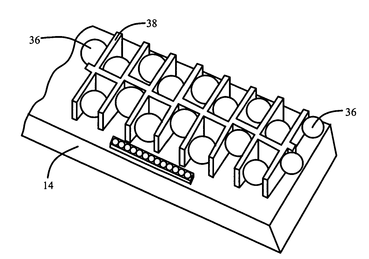
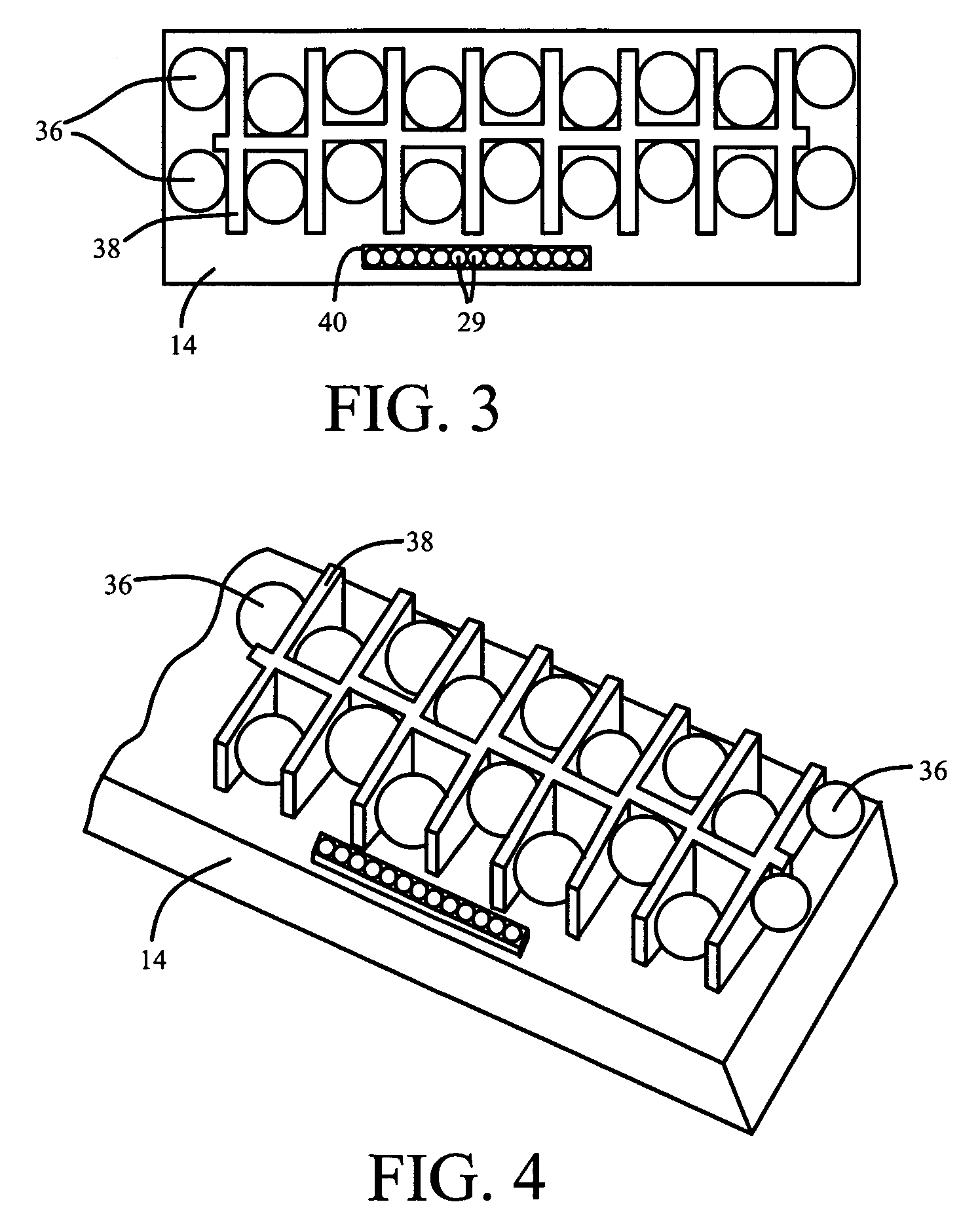
[0032]FIG. 5 is a schematic view of an elastic averaging alignment arrangement that uses both fixed alignment features and flexible alignment features. In this embodiment, the compliance is provided by standoffs 42, 44 and 46 that support solder bumps 48, 50 and 52 above the surface of the substrate 14. The standoffs may be made of polyimide or a similar material having compliancy. The fixed alignment features are downwardly depending regions 54, 56, 58 and 60 of the coupler block 12. In linking the coupler block to the substrate, the spaces between the downwardly depending regions are aligned with the solder bumps. Because the solder bumps are supported by compliant columns (standoffs), the inexactness of positional tolerances in fabricating the coupler block and the standoffs will not prevent seating of the coupler block. By providing sufficient overconstraint, the composite error is well within acceptable limits. Preferably, there are at least twenty standoffs.

third embodiment

[0033]FIG. 6 is a representation of the invention. Within the substrate 14, openings 62, 64, 66 and 68 are formed in positions to receive compliant protrusions 70, 72, 74 and 76 extending from the coupler block 12. This embodiment is less suited for applications in which the substrate is a printed circuit board, since typical hole tolerances for printed circuit boards are too inexact for all but the least demanding alignments. However, the application is well suited for use with flex substrates, ceramic substrates, and particularly semiconductor substrates. When the compliant protrusions are inserted into the substrate openings, the beam ports along a surface of the coupler block are properly aligned with the lenses / active optical elements of the device 40. Alternatively, the compliant protrusions may be formed along the substrate 14, while the openings are formed within the coupler block 12.

[0034]The uses of semiconductor substrates lend themselves particularly well to elastic aver...


PUM


Abstract

In an optoelectronic assembly in which one or more beam paths are to be aligned with a corresponding number of active optical elements, the cooperation between flexible alignment features and fixed alignment features achieves elastic averaging so as to provide the target accuracy. By averaging dimensional and positional errors over a large number of localized couplings of the flexible and fixed alignment features, elastic averaging provides the same accuracy as the more costly and complex kinematic alignment techniques.

Description

BACKGROUND ART[0001]In optoelectronic applications, there is a conversion between an electrical mode and an optical mode of signal communication. In a conversion from the electrical mode, the electrical element is a light source, such as a Vertical Cavity Surface Emitting Laser (VCSEL) or a Light Emitting Diode (LED). On the other hand, a conversion to the electrical mode utilizes a detector as the active optical element.[0002]Optoelectronic modules are often used in coupling system components and to provide the mode conversion. The modules are designed to present a relatively small area along a surface of the module that receives optical fibers and to require a relatively small amount of real estate of a printed circuit board against which another surface of the module is seated. This allows a sequence of optoelectronic modules to be seated in a closely spaced arrangement for parallel handling of a large number of optical signals. Typically, each module includes an array of light s...

Claims


Application Information

Patent Timeline
Patent Type & Authority Patents(United States)
IPC IPC(8): G02B6/26G02B6/12G02B6/42
CPCG02B6/423G02B6/4232G02B6/4214G02B6/4246H01L27/00
Inventor YI, ROBERT H.BAUGH, BRENTON A.WILLIAMS, JAMES H.WILSON, ROBERT E.RUH, RICHARD A.
Owner BROADCOM INT PTE LTD
Why Eureka
Try Eureka