Manufacturing method of semiconductor device

a manufacturing method and semiconductor technology, applied in the direction of semiconductor devices, electrical equipment, basic electric elements, etc., can solve the problems of increased cost, physical strength damage, and difficulty in reusing substrates, and achieve the effect of low cost and high reliability

Inactive Publication Date: 2008-12-16
SEMICON ENERGY LAB CO LTD
View PDF36 Cites 81 Cited by
  • Summary
  • Abstract
  • Description
  • Claims
  • Application Information

AI Technical Summary

Benefits of technology

[0039]According to the invention, when a semiconductor device is used as an element forming layer, a semiconductor device provided over a thin flexible substrate can be provided at low cost, ultimately. In addition, according to the manufacturing method of a semiconductor device of the invention, a semiconductor device with high reliability can be obtained.

Problems solved by technology

However, the methods of removing a supporting substrate by grinding, polishing, or dissolving cause problems like damage due to physical strength such as stress and vibration, and contamination.
Furthermore, according to such methods, it is quite difficult to reuse a substrate and the cost is increased.
In addition, in the case where an element forming layer constituted by a thin film transistor and the like is provided over a peeling layer, the property of the transistor may be affected and the reliability of a semiconductor device may be decreased depending on a material or the film quality of the peeling layer.

Method used


Image

  • Manufacturing method of semiconductor device
  • Manufacturing method of semiconductor device
  • Manufacturing method of semiconductor device

Examples


embodiment mode 1

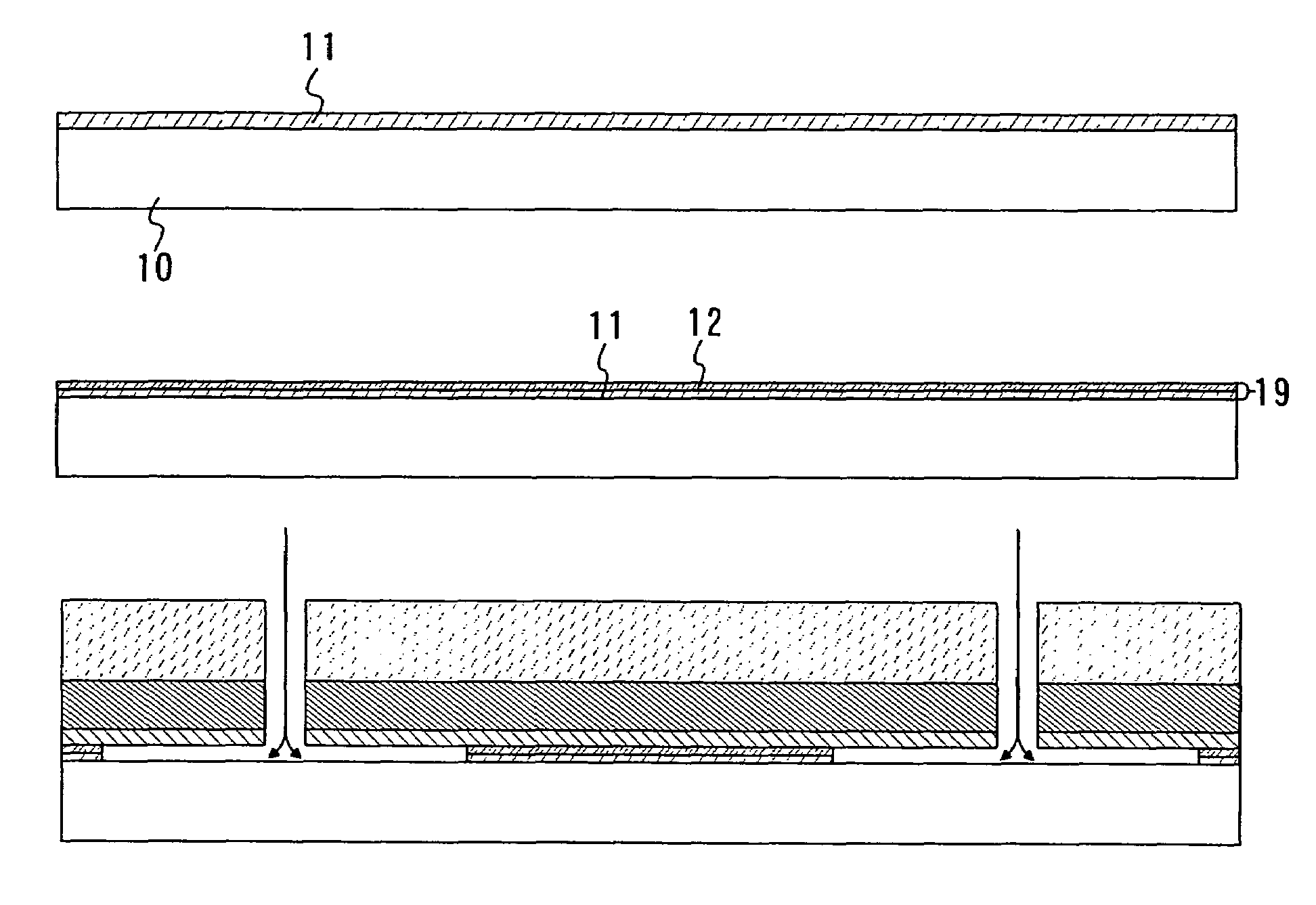
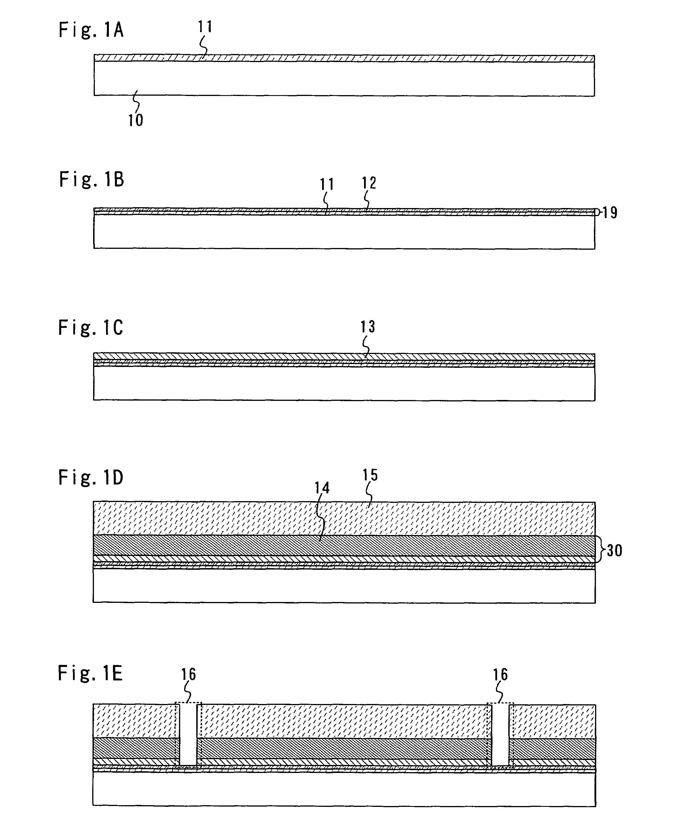
[0073]In this embodiment mode, one example of a manufacturing method of a semiconductor device of the invention is described with reference to drawings.

[0074]First, a metal film 11 is formed on a surface of a substrate 10 (FIG. 1A). The metal film 11 may be formed as a single layer or a plurality of layers laminated. For example, a tungsten (W) film is formed by a sputtering method. It is to be noted that an insulating film may be provided over the substrate 10 before the metal film 11 is formed. In particular, it is preferable to provide an insulating film between the substrate 10 and the metal film 11 when the contamination from the substrate may occur.

[0075]Next, a plasma treatment is applied to the metal film 11 in an atmosphere of dinitrogen monoxide alone or a mixture gas atmosphere of dinitrogen monoxide and another gas to form a film 12 made of metal oxide, metal nitride or metal nitride oxide on a surface of the metal film 11 (FIG. 1B). The film 12 made of metal oxide, meta...

embodiment mode 2

[0097]In this embodiment mode, a manufacturing method of a semiconductor device different from the above embodiment mode is described with reference to drawings.

[0098]First, the metal film 11 is formed on a surface of the substrate 10 (FIG. 4A). The metal film 11 may be formed as a single layer or a plurality of layers laminated. For example, a tungsten (W) film is formed by a sputtering method. It is to be noted that an insulating film may be provided over the substrate 10 before the metal film 11 is formed. In particular, it is preferable to provide an insulating film between the substrate 10 and the metal film 11 when the contamination from the substrate may occur.

[0099]Next, in this embodiment mode, a heat treatment using RTA or an annealing furnace is performed to oxidize, nitride or nitride oxidize the metal film 11 in an atmosphere of dinitrogen monoxide alone or a mixture gas atmosphere of dinitrogen monoxide and another gas, so that a film 22 made of metal oxide, metal nitr...

embodiment mode 3

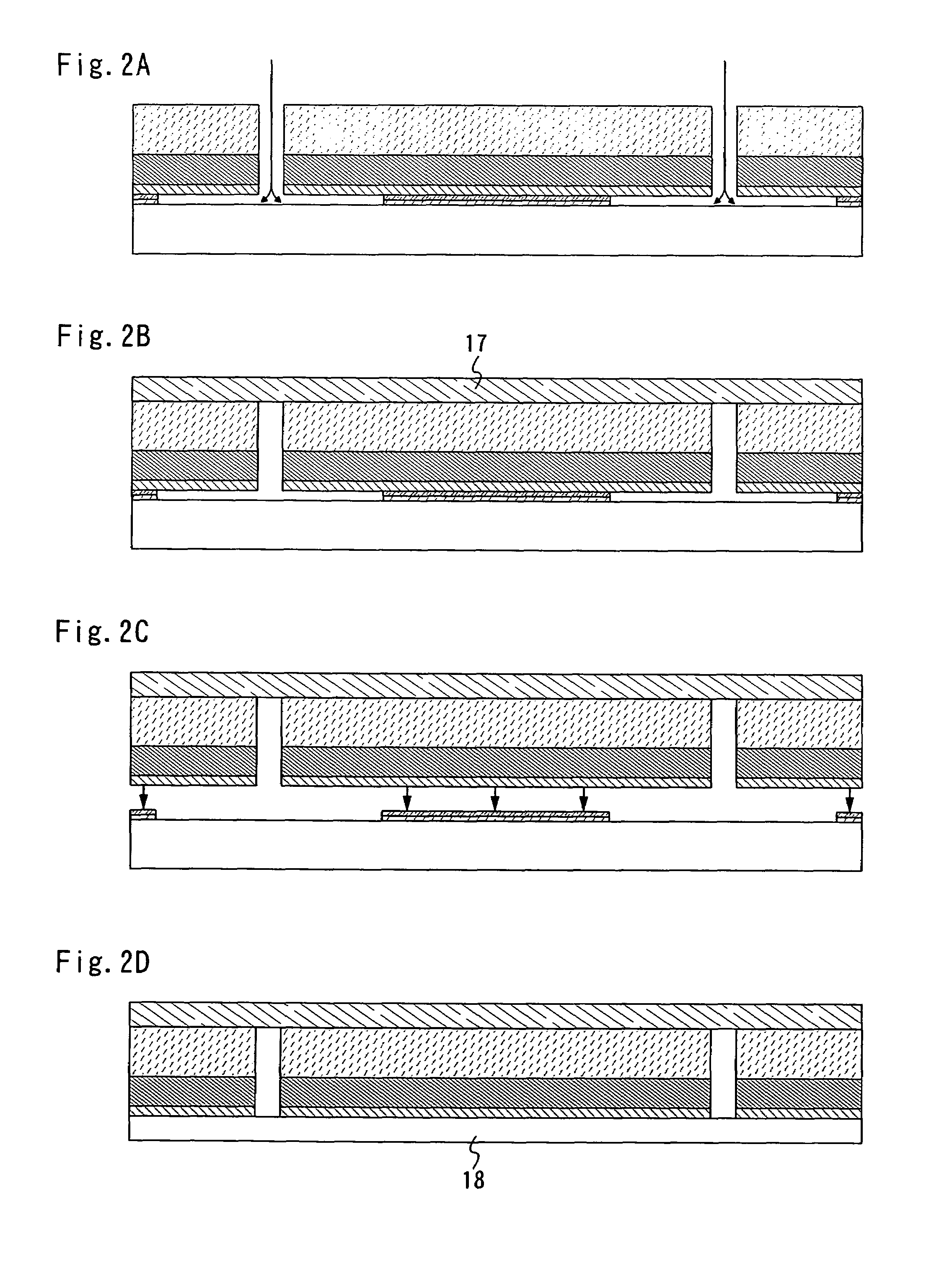
[0104]In this embodiment mode, a manufacturing method of a semiconductor device different from the above embodiment modes is described with reference to drawings.

[0105]First, a film 29 made of metal oxide, metal nitride or metal nitride oxide is formed on a surface of the substrate 10 by a sputtering method in an atmosphere of dinitrogen monoxide alone or a mixture gas atmosphere of dinitrogen monoxide and another gas (FIG. 5A). For example, the sputtering is performed using tungsten as a target in an atmosphere of dinitrogen monoxide alone or a mixture gas atmosphere of dinitrogen monoxide and argon to form a film made of tungsten oxide (WOx), tungsten nitride (WNx) or tungsten nitride oxide (WNxOy) over the substrate 10. Besides tungsten, the film 29 made of metal oxide, metal nitride or metal nitride oxide may be formed as a single layer or a laminated layer of a film using an element selected from molybdenum (Mo), titanium (Ti), tantalum (Ta), niobium (Nb), nickel (Ni), cobalt (...


PUM

PropertyMeasurementUnit
temperatureaaaaaaaaaa
thicknessaaaaaaaaaa
thicknessaaaaaaaaaa

Abstract

An object of the present invention is to provide a method for manufacturing a semiconductor device with high reliability, at low cost, in which an element forming layer having a thin film transistor and the like provided over a substrate is peeled from the substrate, so that a semiconductor device is manufactured. According to the invention, a metal film is formed over a substrate, a plasma treatment is performed to the metal film in a dinitrogen monoxide atmosphere to form a metal oxide film over the metal film, a first insulating film is formed continuously without being exposed to the air, an element forming layer is formed over the first insulating film, and the element forming layer is peeled from the substrate, so that a semiconductor device is manufactured.

Description

BACKGROUND OF THE INVENTION[0001]1. Field of Invention[0002]The present invention relates to a manufacturing method of a semiconductor device, and particularly to a method for manufacturing a semiconductor device in which an element forming layer is peeled off a supporting substrate by using a peeling layer provided between the supporting substrate and the element forming layer.[0003]2. Description of the Related Art[0004]In recent years, the necessity of a card mounting an RFID (Radio Frequency Identification) or a tag mounting an RFID which can transmit and receive data without contact has been increased in any fields which need automatic identification such as management of valuable securities and merchandise. The card mounting an RFID reads and writes data from / to an external device via a loop antenna in the card without contact. The card mounting an RFID has larger memory capacity and higher security than a magnetic card that records data by a magnetic recording method. Hence, ...

Claims


Application Information

Patent Timeline
Patent Type & Authority Patents(United States)
IPC IPC(8): H01L21/311
CPCH01L21/7806H01L27/1214H01L27/1266
Inventor TAMURA, TOMOKOOGITA, KAORIDAIRIKI, KOJIMARUYAMA, JUNYA
Owner SEMICON ENERGY LAB CO LTD
Why Eureka
Try Eureka