Communication semiconductor integrated circuit, radio communication system, and adjustment method of gain and offset

a technology of integrated circuits and semiconductors, applied in the field of communication semiconductor integrated circuits, radio communication systems, and adjustment methods of gain and offset, can solve the problems of circuit dimensions increasing, little time is allowed for d.c. offset cancellation, and difficult application to a wireless lan system, etc., and achieve accurate level measurement

Inactive Publication Date: 2008-12-30
RENESAS ELECTRONICS CORP
View PDF7 Cites 9 Cited by
  • Summary
  • Abstract
  • Description
  • Claims
  • Application Information

AI Technical Summary

Benefits of technology

[0018]The means described above, since it need not detect the D.C. offsets of the amplifiers at the time of starting reception and can cancel the D.C. offsets of the amplifiers with offset cancellation values, offset cancellation is completed in a short period of time. Further in the plurality of variable gain amplifiers, though the D.C. offset differs with the set gain, i.e. with the amplifier used, by storing the D.C. offset cancellation values of the amplifiers in the memory according to set gains, it is enabled to immediately cancel, when the gain is altered, the D.C. offset of the amplifier according to the pertinent offset cancellation value stored in the memory.
[0019]Further, where the high gain amplifier circuit for amplifying reception signals to a predetermined amplitude level consist of a plurality of variable gain amplifiers connected in multiple stages, a variable gain amplifier at a prior stage cancels a D.C. offset according to an offset cancellation value read out of a memory, and D.C. offset cancellation by the variable gain amplifier at the final stage is accomplished on a real time basis after the completion of offset cancellation by the prior variable gain amplifier. This makes possible prompt and highly precise D.C. offset correction because rough D.C. offset cancellation is executed in the very short period of time allowed at the start of reception and D.C. offset cancellation of the whole reception circuit, covering the residual offset of the prior variable gain amplifier as well, is subsequently carried out.
[0020]Preferably, as the offset canceling circuit here, a circuit comprising an A / D converter for A / D conversion of the outputs of amplifiers and a D / A converter for D / A conversion of values canceling the detected offsets and so configured as to determine offset cancellation values by consecutive comparing actions by the A / D converter should be used. Such a circuit, as the A / D converter therein can be configured of a comparator and a simple circuit, such as a resistor voltage divider circuit to give voltages to be compared to the comparator, can be reduced in circuit dimensions.
[0021]According to a second aspect of the invention under the present application, the gain of a high gain amplifier circuit for amplifying reception signals into signals of a predetermined amplitude level is set in two steps of rough setting and precise setting on the basis of the detection of the level of the reception signals by a measuring circuit. The output of the level measuring circuit is made to pass an averaging filter of which the length of time taken by a signal at the input end to appear at the output end is set equal to the period of the reception signals to be measured and, after detecting that the signal having passed the averaging filter has reached or surpassed a predetermined level, the output level of the averaging filter after the lapse of the same length of time as the period of the reception signals is treated as the measured level. This makes it possible to detect the entrance of the reception signals in a short period of time after the start of reception, and to obtain the result of accurate level measurement of those reception signals without delay.

Problems solved by technology

For this reason it has been revealed that, though this formula is applicable to a radio communication system, such as a cellular phone, in which there is little hurry at the time of reception start, its application is difficult to a wireless LAN system in which little time is allowed for D.C. offset cancellation.
On the other hand, as the formula described in Patent Reference 2 by which D.C. offsets are detected from carrier leaks, a modulator for re-modulating I and Q signals demodulated from reception signals and a carrier leak detecting circuit are additionally required, the circuit dimensions will increase and, moreover, errors may occur in the modulator and the carrier leak detecting circuit.

Method used


Image

  • Communication semiconductor integrated circuit, radio communication system, and adjustment method of gain and offset
  • Communication semiconductor integrated circuit, radio communication system, and adjustment method of gain and offset
  • Communication semiconductor integrated circuit, radio communication system, and adjustment method of gain and offset

Examples


Embodiment Construction

[0040]Next will be described a preferred embodiment of the present invention with reference to the accompanying drawings.

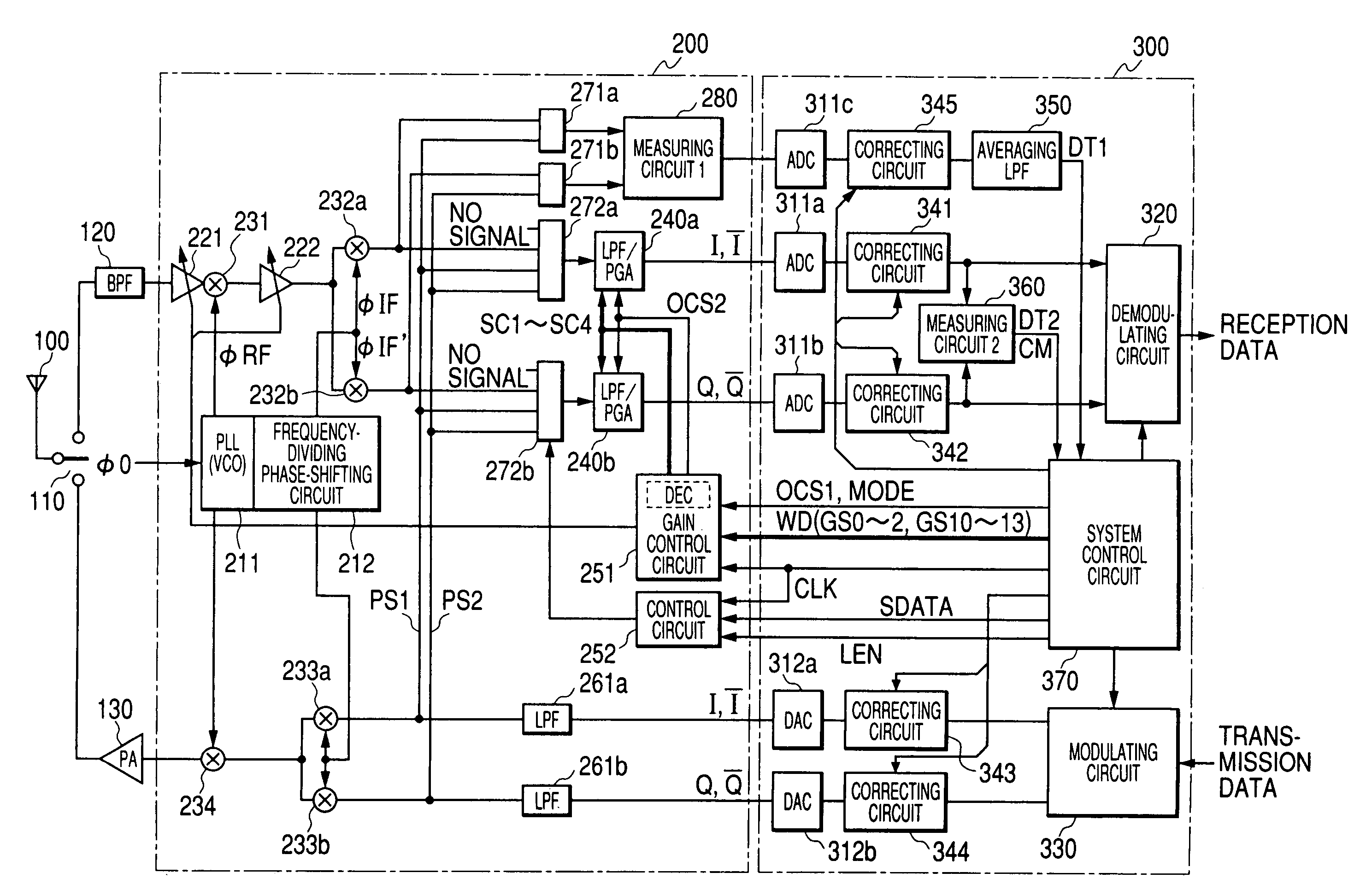
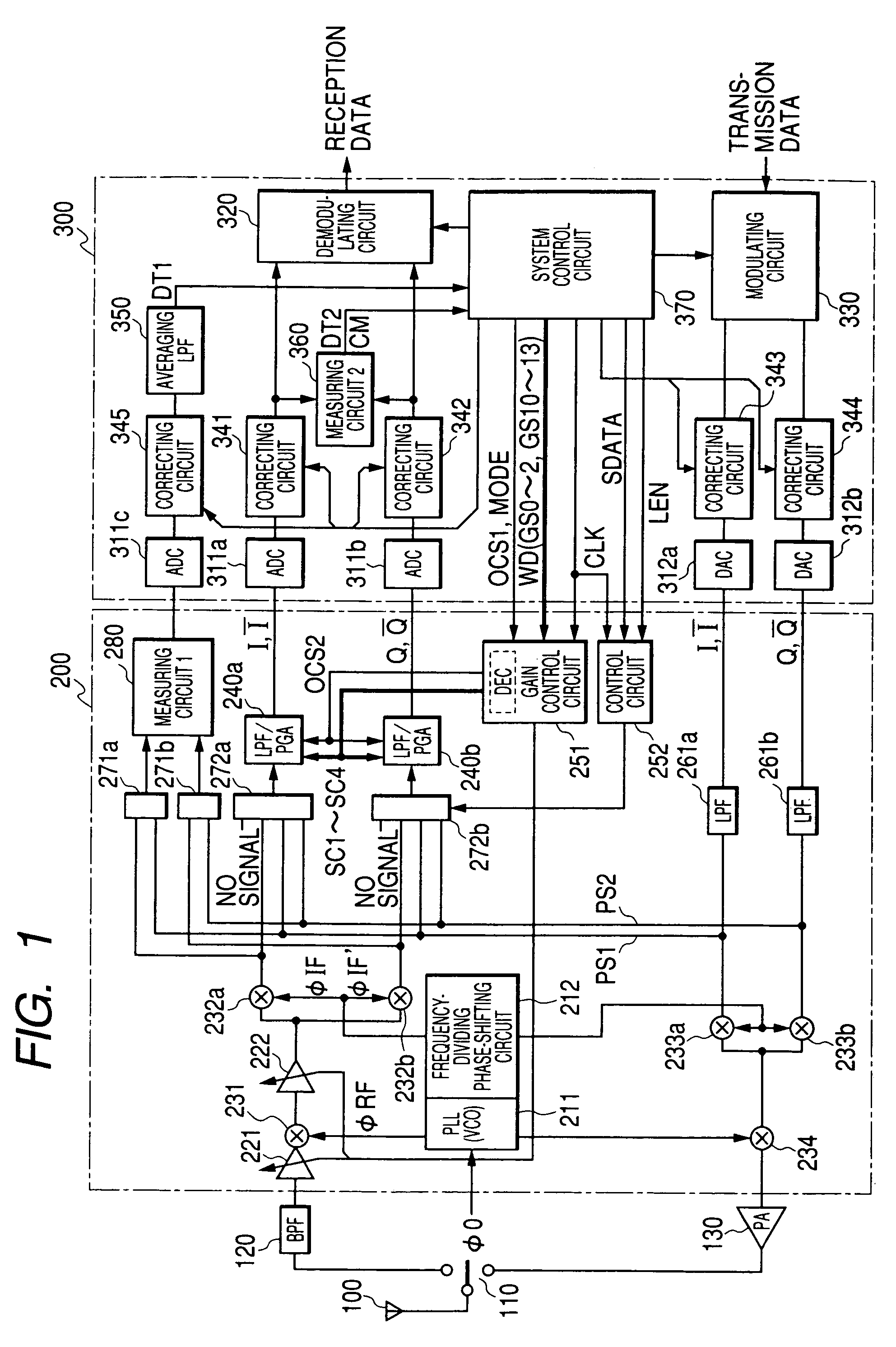
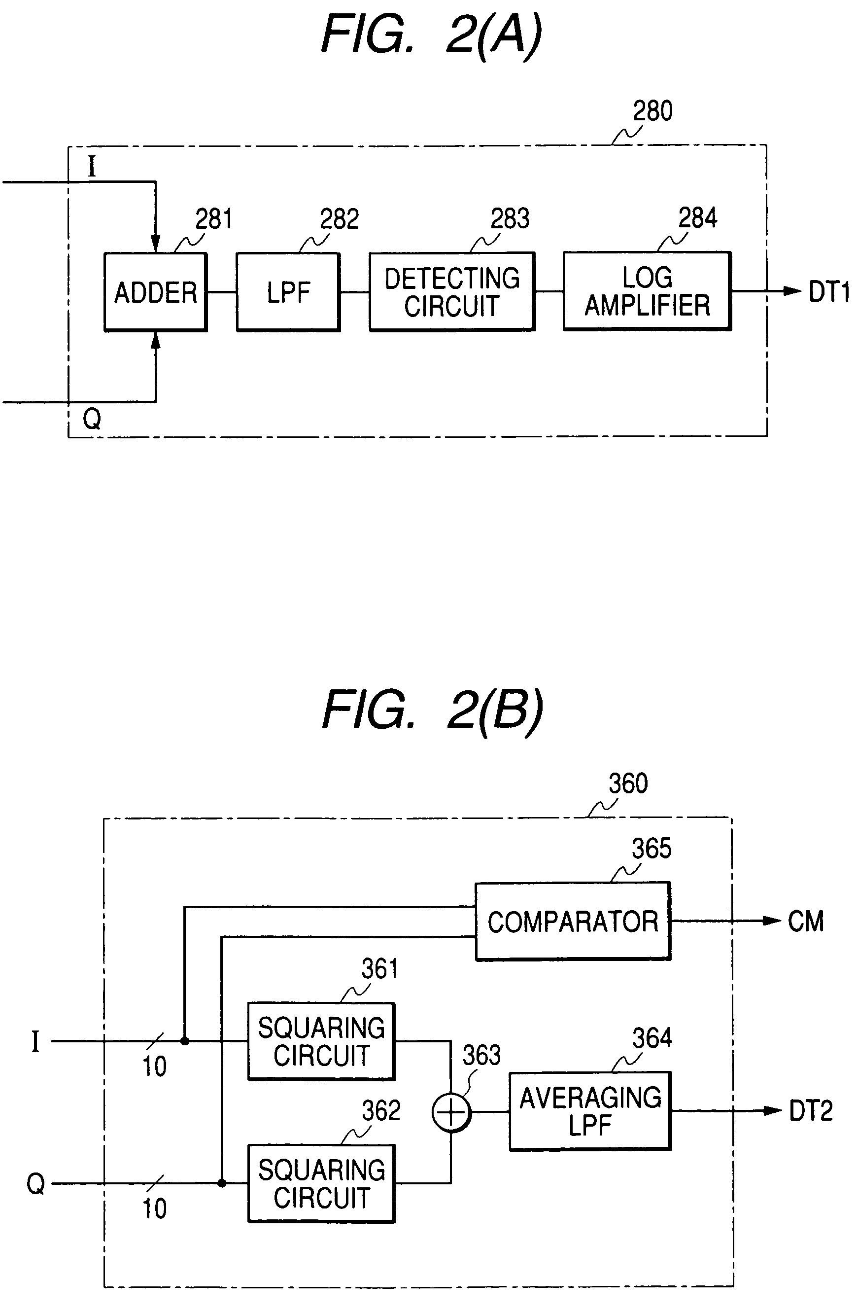
[0041]FIG. 1 is a block diagram showing a radio communication system to which the present invention can be suitably applied and an example of configuration of a high frequency IC and a baseband LSI constituting the system.

[0042]The radio communication system, which embodies the invention in this manner, comprises an antenna 100 for transmitting and receiving signal waves, a switch 110 for changing over between transmission and reception, a band-pass filter 120 for removing unnecessary waves from reception signals, a power amplifier 130 for amplifying the power of transmission signals and transmitting them from the antenna 100, a high frequency IC 200 for down-converting reception signals and up-converting transmission signals, and a baseband LSI 300 performing modulation / demodulation and baseband processing.

[0043]FIG. 1 illustrates the system in a simplified way e...


PUM


Abstract

A D.C. offset canceling technique and a gain adjusting technique permitting completion of correction of D.C. offsets and gain adjustment of amplifiers for amplifying reception signals in a relatively short period of time in a radio communication system, such as a wireless LAN, are to be provided. A communication semiconductor integrated circuit (high frequency IC) has a plurality each of low-pass filters and variable gain amplifiers which are alternately connected in multiple stages, and high gain amplifier circuits for amplifying reception signals to a predetermined amplitude level while eliminating unnecessary waves. Offset cancellation values are generated by detecting in advance D.C. offsets of amplifiers for amplifying reception signals according to a set gain, and stored into a memory, and read out of the memory to cancel the D.C. offsets of the amplifiers at the time of starting reception and altering the gain. Gain setting in a high gain amplifying section for amplifying reception signals is accomplished in two steps, rough setting and precise setting.

Description

CROSS-REFERENCE TO RELATED APPLICATION[0001]The present application claims priority from Japanese patent application No. JP 2003-178984 filed on Jun. 24, 2003, the content of which is hereby incorporated by reference into this application.BACKGROUND OF THE INVENTION[0002]The present invention relates to a technique that can be effectively applied to the correction of D.C. offsets and the adjustment of gains in a variable gain amplifier circuit provided in the reception circuitry of a radio communication system and to a high gain amplifier circuit which successively amplifies reception signals with a plurality of amplifier circuits in multiple stage connection, for instance a technique that can be effectively utilized in a wireless local area network (LAN) system and high frequency semiconductor integrated circuits (ICs) and baseband large scale integrated circuits (LSIs) used therein.[0003]A wireless LAN system or a cellular phone is usually provided with a high gain amplifier circu...

Claims


Application Information

Patent Timeline
Patent Type & Authority Patents(United States)
IPC IPC(8): H04L27/08H03G3/20H03G3/30H04B1/30H04J11/00H04L25/06H04L27/22H04L27/26H04L27/38
CPCH03G3/3068H04L25/061H04L27/3809H04L27/2647
Inventor HABUKA, TOSHIHITOINOKAWA, NAOTOOZAKI, KIYOHARUMATSUURA, TATSUJIYAHAGI, KOICHI
Owner RENESAS ELECTRONICS CORP
Why Eureka
Try Eureka