

Connector assembly with integrated electromagnetic shield
a technology of electromagnetic shielding and connector assembly, applied in the field of electromagnetic shielding, can solve the problems of introducing bit errors on the link, affecting the operation of the link, so as to achieve the effect of higher levels of radiated nois
- Summary
- Abstract
- Description
- Claims
- Application Information
AI Technical Summary
Benefits of technology
Problems solved by technology
Method used
Image

Examples
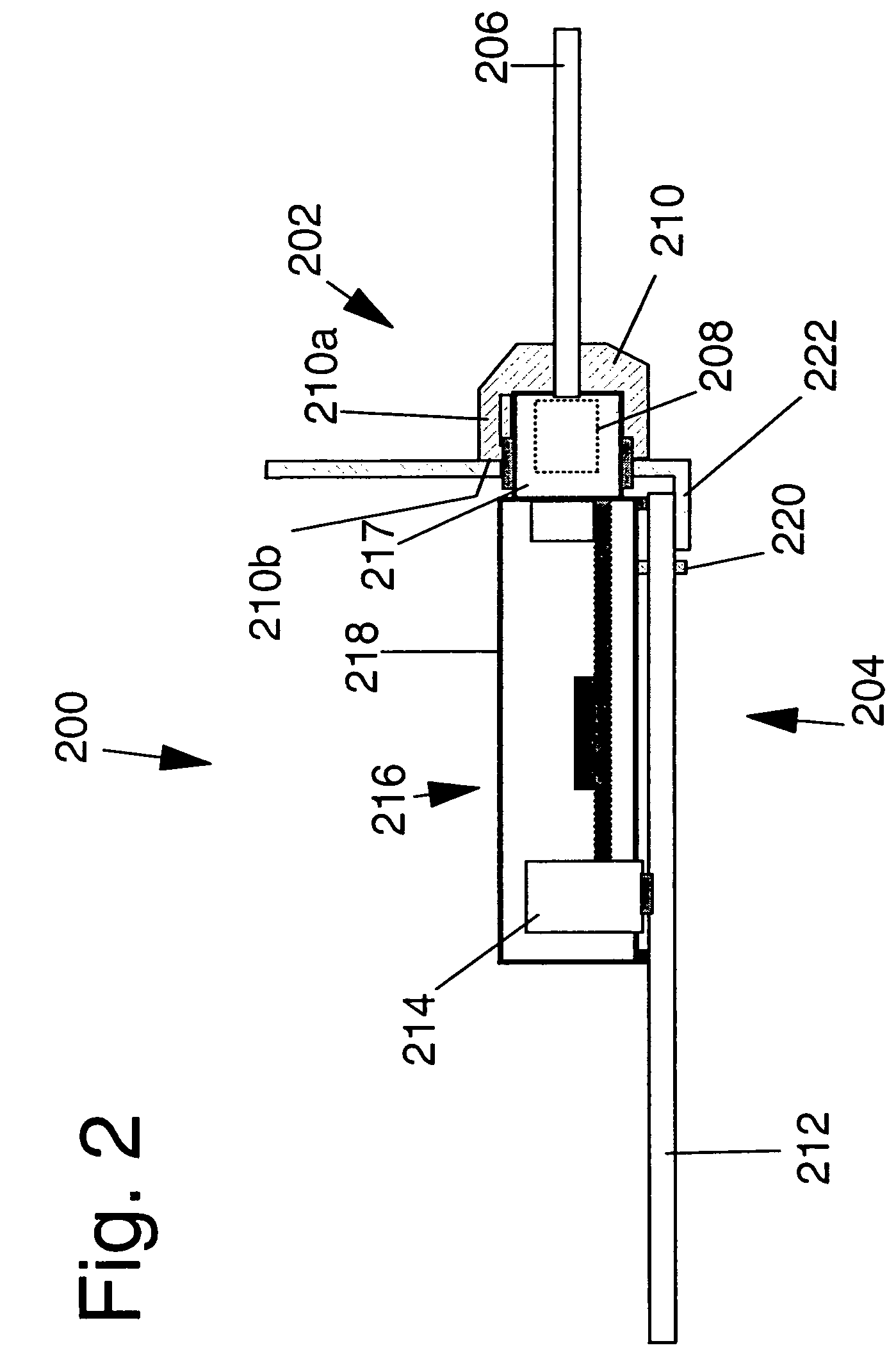
embodiment 200
[0033]FIG. 2 illustrates one example of a preferred embodiment 200 in which a fiber optic cable assembly 202 connects to a card assembly 204. Cable assembly 202 comprises a fiber optic cable 206 having a connector 208 as well as the boot of the present invention, to be described below. Except for the boot, cable assembly 202 is of conventional design.
[0034]Card assembly 204, which is likewise of conventional design, comprises a printed wiring board (PWB) 212 which carries a surface mount technology (SMT) connector 214 for receiving a pluggable optical transceiver 216 with a parallel interface; “parallel” here refers not to the electrical interface, but to the fact that transceiver 216 transmits and receives optical streams over a plurality of channels (not separately shown), which are typically displaced from one another in the direction of the view. Optical transceiver 216 has a receptacle 217 at one end for receiving the connector 208. Connector 208 and receptacle 217 are each for...
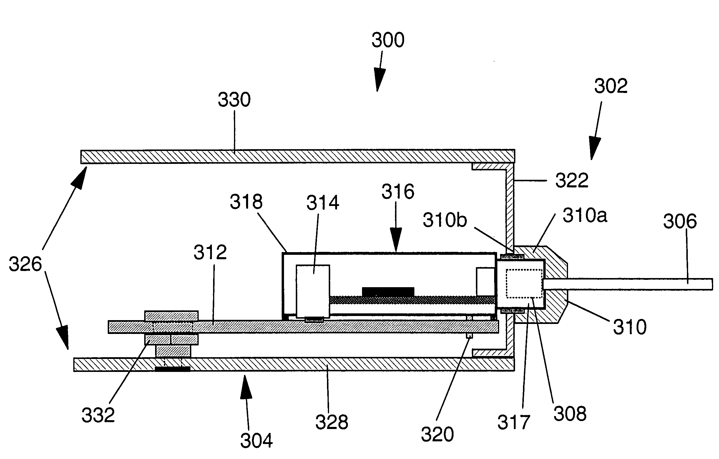
embodiment 300
[0037]The embodiment 300 shown in FIG. 3 serves to seal the one remaining aperture (the opening in tailstock 322 for receptacle 317) in the enclosure 326 (through the mating of the boot 310 with the tailstock 322), such that a complete Faraday shield is created around the optical transceiver components. It will be apparent to those skilled in the art that variations of this approach are applicable to both parallel optical interfaces, such as pluggable InfiniPak-compliant modules, and serial interfaces, such as small-form-factor pluggable (SFP) compliant modules.
[0038]FIG. 4 illustrates one example of a cable-to-cable connection 400 between a first cable assembly 402 and a second cable assembly 404. Cable assembly 402 comprises a cable 406 having a connector 408 fitted with a cable boot 410, while cable assembly 404 similarly comprises a cable 412 having a connector 414 fitted with a cable boot 416. Connector 414 is a male connector having a reduced-diameter projecting portion 415, w...
PUM
 Abstract
Description
Claims
Application Information