VCSEL for high speed lower power optical link

a technology of optical link and vcsel, which is applied in the direction of semiconductor lasers, lasers, electrical equipment, etc., can solve the problems of long-wavelength vcsels that require newer materials, optical loss, and vcsels similar to those illustrated in fig. 1 that have problems, etc., and achieves reduced power, large optical modulation amplitude, and reduced power

Inactive Publication Date: 2009-03-10
IBM CORP
View PDF5 Cites 16 Cited by
  • Summary
  • Abstract
  • Description
  • Claims
  • Application Information

AI Technical Summary

Benefits of technology

[0009]The present invention solves the problems of prior art methods of producing VCSEL chips. It is an objective of the present invention to provide a VCSEL design to achieve a power reduction in a high-speed optical interconnect. In order to realize a low power optical interconnect, the VCSEL according to an exemplary embodiment of the present invention for use with an optical interconnect emits larger optical modulation amplitude (OMA) at high data rate with smaller modulation current (IMOD) and lower bias current (Ib). Low threshold material gain (gth) reduces Ib required for high modulation bandwidth. High differential quantum efficiency (DQE) provides larger OMA with smaller IMOD, as well as reduces Ib required for OMA. Low series resistance (RS) decreases both modulation (VMOD) and bias (Vb) voltages. The VCSEL with gth<1000 cm−1, DQE>50%, and RS<100 Ω provides an optical interconnect transmitter operating at 15 Gbps with the OMA of over −1 dBm and the power dissipation of less than 10 mW. The present invention provides the design of a VCSEL which achieves gth<1000 cm−1, DQE>50%, and RS<100 Ω. The gth of the VCSEL is reduced by increasing the reflectivity (R) of its distributed Bragg reflector (DBR) mirrors, although the increased R decreases the DQE. A tunnel junction enables the elimination of all p-type layers in the VCSEL except the tunnel junction itself by altering the p-layers to n-type. The same doping level results in a factor of 2 smaller free-carrier optical absorption at the wavelength of about 850-1000 nm for n-type than for p-type. High mobility of...

Problems solved by technology

Long-wavelength VCSELs require newer materials and/or more complicated structures mainly lack of optimum material systems providing high DBR mirror reflectivity and high material gain at the same time.
While...

Method used


Image

  • VCSEL for high speed lower power optical link
  • VCSEL for high speed lower power optical link
  • VCSEL for high speed lower power optical link

Examples


Embodiment Construction

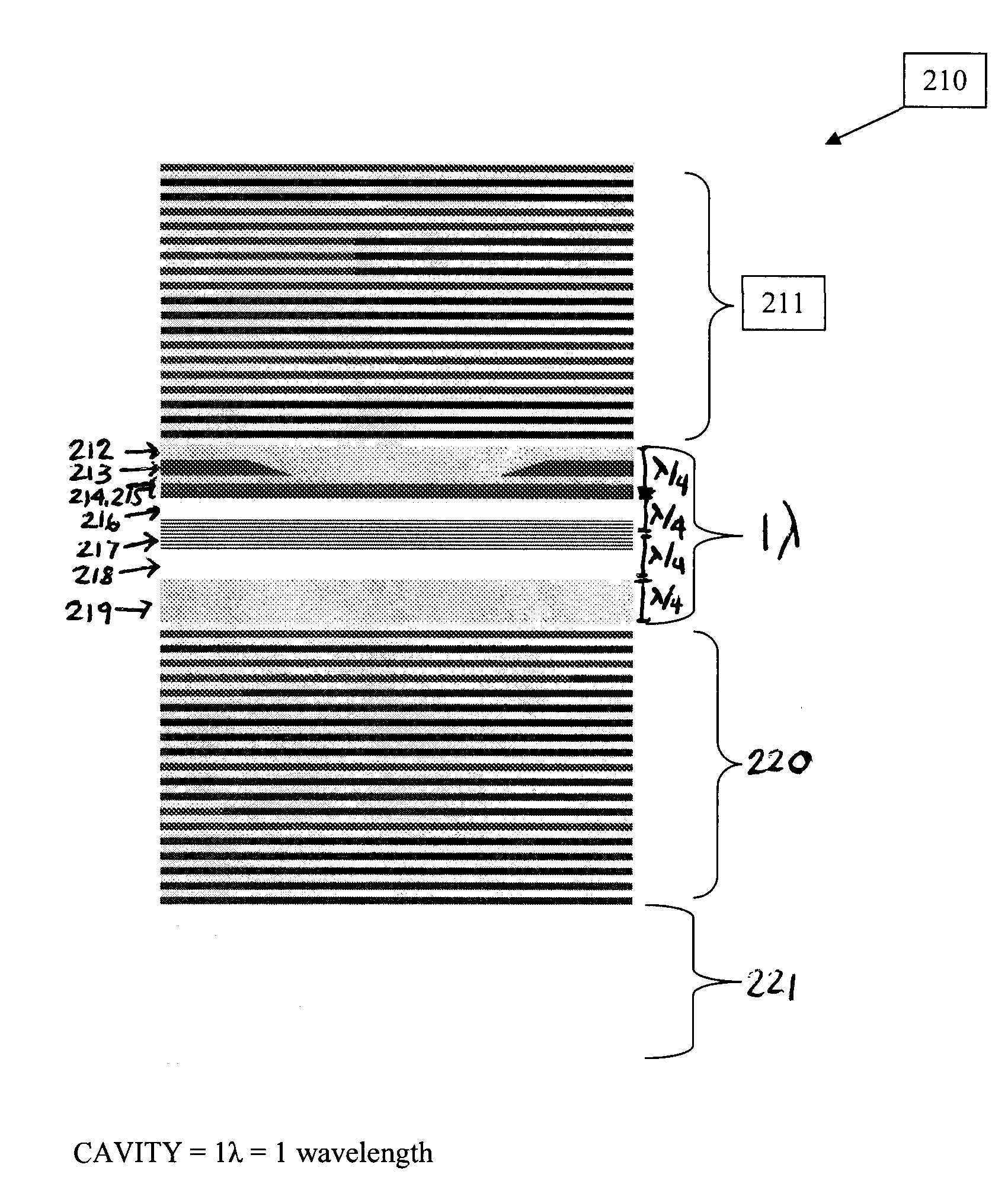
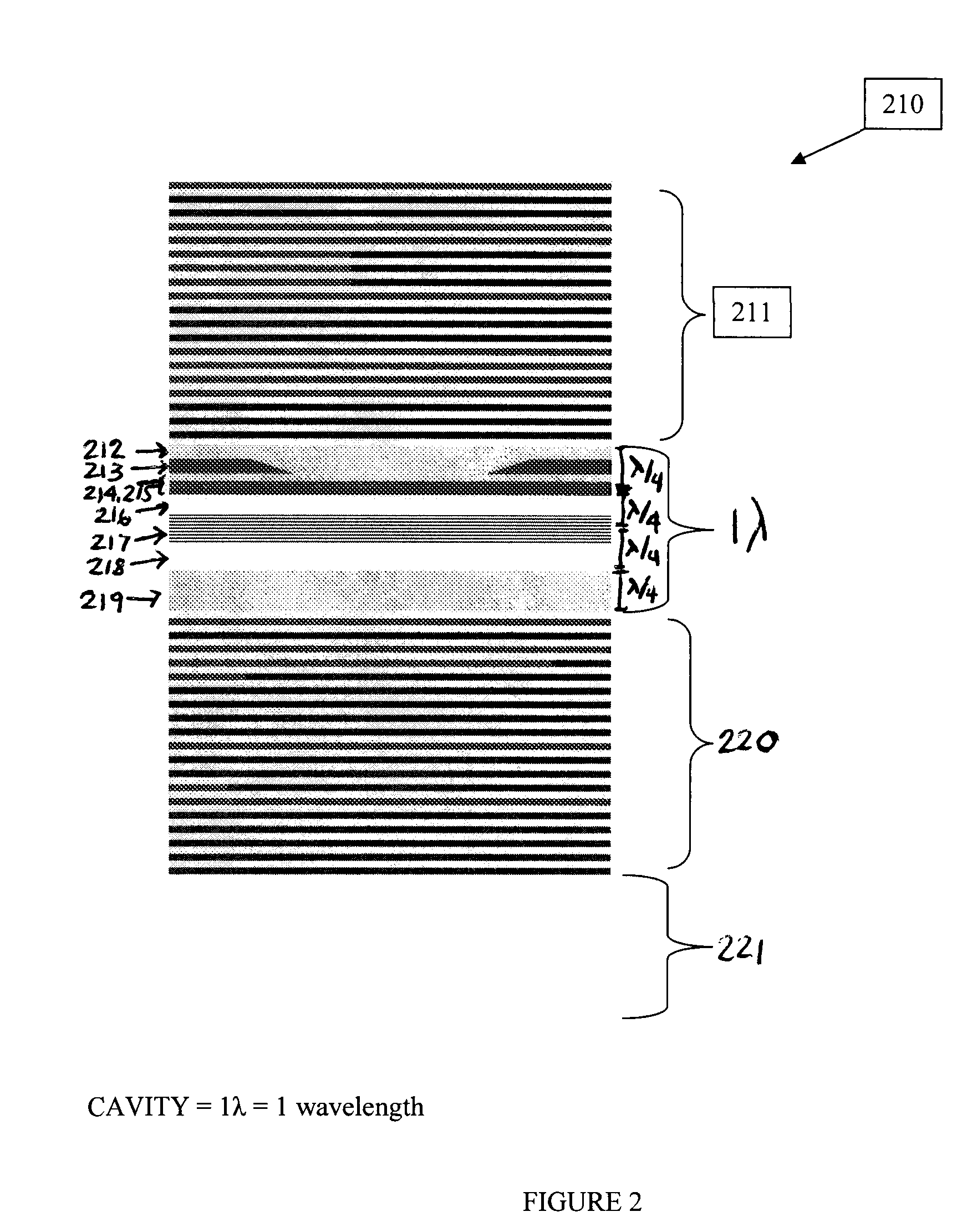
[0014]An exemplary embodiment of a VCSEL, also called coherent light generators, for low power high speed optical interconnect emitting at the wavelength of around 980 nm is shown in FIG. 2. This embodiment is for illustration purposes only. The present invention is not limited this embodiment as those skilled in the art will recognize the layers may be modified from those shown with departing from the spirit of the invention. Further, the wavelength is not limited to 980 nm, and can be applied to 850 nm or even longer wavelength over 1000 nm. The present invention may be modified to operate at any wavelength including UV, visible and IR. The following discussion is made in reference to FIG. 2.

[0015]Top (DBR1) 211 and bottom (DBR2) 220 are preferably comprised of alternating Al0.85Ga0.15As and GaAs layers. Their reflectivity is R1 and R2, respectively. One-lambda (wavelength, i.e. 980 nm in this case) thick optical cavity is located between the 211 and 220. Lambda / 4 thick upper an...


PUM


Abstract

A method of manufacturing a coherent light generator, especially a vertical cavity surface emitting laser (VCSEL), includes a gallium based semiconductor alloy substrate, a first DBR stack over the substrate, a first n-type clad layer over the first DBR stack, an active region containing quantum wells over the first n-type clad, a tunnel junction having an n-type and a p-type material and a boundary over the active region so that there is a standing wave null at an operating wavelength at the n-type/p-type boundary in the tunnel junction, a second n-type clad layer over the tunnel junction, an oxide aperture at least partially installed in the second n-type clad layer, and the second DBR stack over the second n-type clad of the coherent light generator. The novel VCSEL provides minimized internal optical absorption and has a low electrical resistance.

Description

FIELD OF THE INVENTION[0001]This invention relates to the vertical cavity surface emitting laser (VCSEL). More specifically, it relates to the VCSEL structure that realizes a low power and high speed appropriate for a high speed optical link.BACKGROUND OF THE INVENTION[0002]Vertical cavity surface emitting lasers (VCSELs) represent a relatively new class of semiconductor lasers. While there are many variations of VCSELs, one common characteristic is that they emit light perpendicular to a wafer's surface. Advantageously, VCSELs can be formed from a wide range of material systems to produce specific characteristics. VCSELs include semiconductor active regions, which can be fabricated from a wide range of material systems, distributed Bragg reflector (DBR) mirrors, current confinement structures, substrates, and contacts. Some VCSELs, particularly those used at long-wavelengths, incorporate tunnel junctions. Because of their complicated structure, and because of their material require...

Claims


Application Information

Patent Timeline
IPC IPC(8): H01L21/20
CPCB82Y20/00H01S5/18311H01S5/18358H01S5/305H01S5/3095H01S5/3211H01S5/34313
Inventor NAKAGAWA, SHIGERU
Owner IBM CORP
Why Eureka
Try Eureka