
Spin-transfer based MRAM with reduced critical current density

a technology of critical current density and mram, applied in the field of spin-transfer-based mram devices, can solve the problems of unintentional alteration of neighboring cells, affecting the stability of neighboring cells,

Active Publication Date: 2009-03-10
EVERSPIN TECHNOLOGIES
View PDF7 Cites 44 Cited by
  • Summary
  • Abstract
  • Description
  • Claims
  • Application Information

AI Technical Summary

Benefits of technology

The present invention relates to magnetic random access memory (MRAM) devices, particularly those that use spin-transfer based techniques for writing data. The technical effects of the invention include improved data retention, reduced power consumption, and compatibility with high-density applications. The invention also provides a method for selectively writing to a designated MRAM cell without affecting the data in other cells. Overall, the invention provides a more efficient and reliable MRAM device.

Problems solved by technology

The traditional MRAM switching technique has some practical limitations, particularly when the design calls for scaling the bit cell to smaller dimensions.
For example, since this technique requires two sets of magnetic field write lines, the array of MRAM cells is susceptible to bit disturbs (i.e., neighboring cells may be unintentionally altered in response to the write current directed to a given cell).
Furthermore, decreasing the physical size of the MRAM free layer results in lower magnetic stability against magnetization switching due to thermal fluctuations.
The stability of the bit can be enhanced by utilizing a magnetic material for the free layer with a large magnetic anisotropy and therefore a large switching field, but then the currents required to generate a magnetic field strong enough to switch the bit are impractical in real applications.
In practice, however, this technique is difficult to implement in a memory array because the write current must flow through the magnetic tunnel junction embodied in the cell.
This negatively affects the reliability of the MRAM cells and requires the use of larger write transistors at each bit location that are capable of producing the necessary currents, which is incompatible with high-density applications.
However, these methods require specific materials for the free layer, which can negatively affect switching reliability and also the read signal.

Method used


Image

  • Spin-transfer based MRAM with reduced critical current density
  • Spin-transfer based MRAM with reduced critical current density
  • Spin-transfer based MRAM with reduced critical current density

Examples


Embodiment Construction

[0017]The following detailed description of the invention is merely exemplary in nature and is not intended to limit the invention or the application and uses of the invention. Furthermore, there is no intention to be bound by any theory presented in the preceding background of the invention or the following detailed description of the invention.

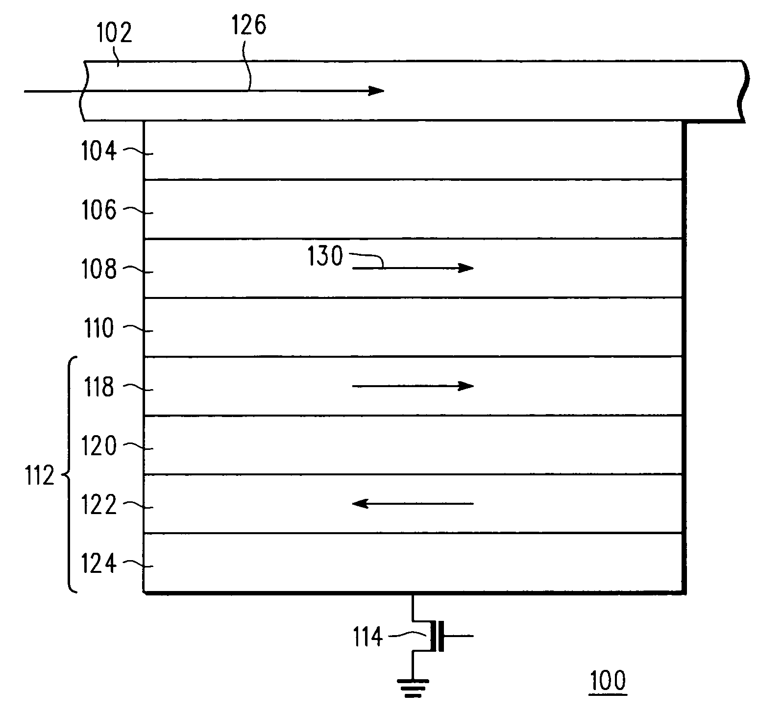
[0018]The spin-transfer effect is known to those skilled in the art. Briefly, a current becomes spin-polarized after the electrons pass through the first magnetic layer in a magnet / non-magnet / magnet trilayer structure, where the first magnetic layer is substantially thicker than the second magnetic layer. The spin-polarized electrons cross the nonmagnetic spacer and then, through conservation of angular momentum, place a torque on the second magnetic layer, which switches the magnetic orientation of the second layer to be parallel to the magnetic orientation of the first layer. If a current of the opposite polarity is applied, the electrons ...


PUM


Abstract

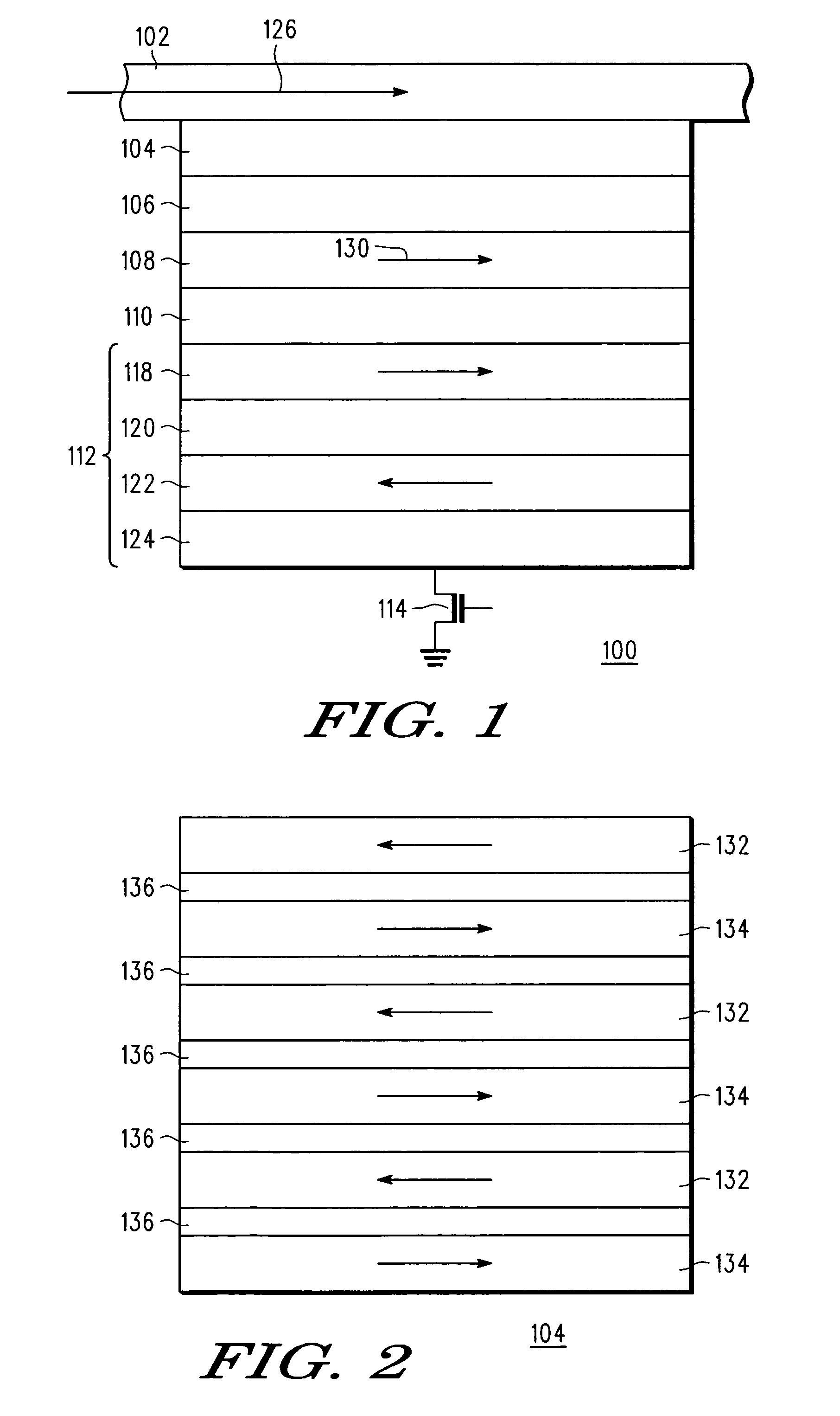
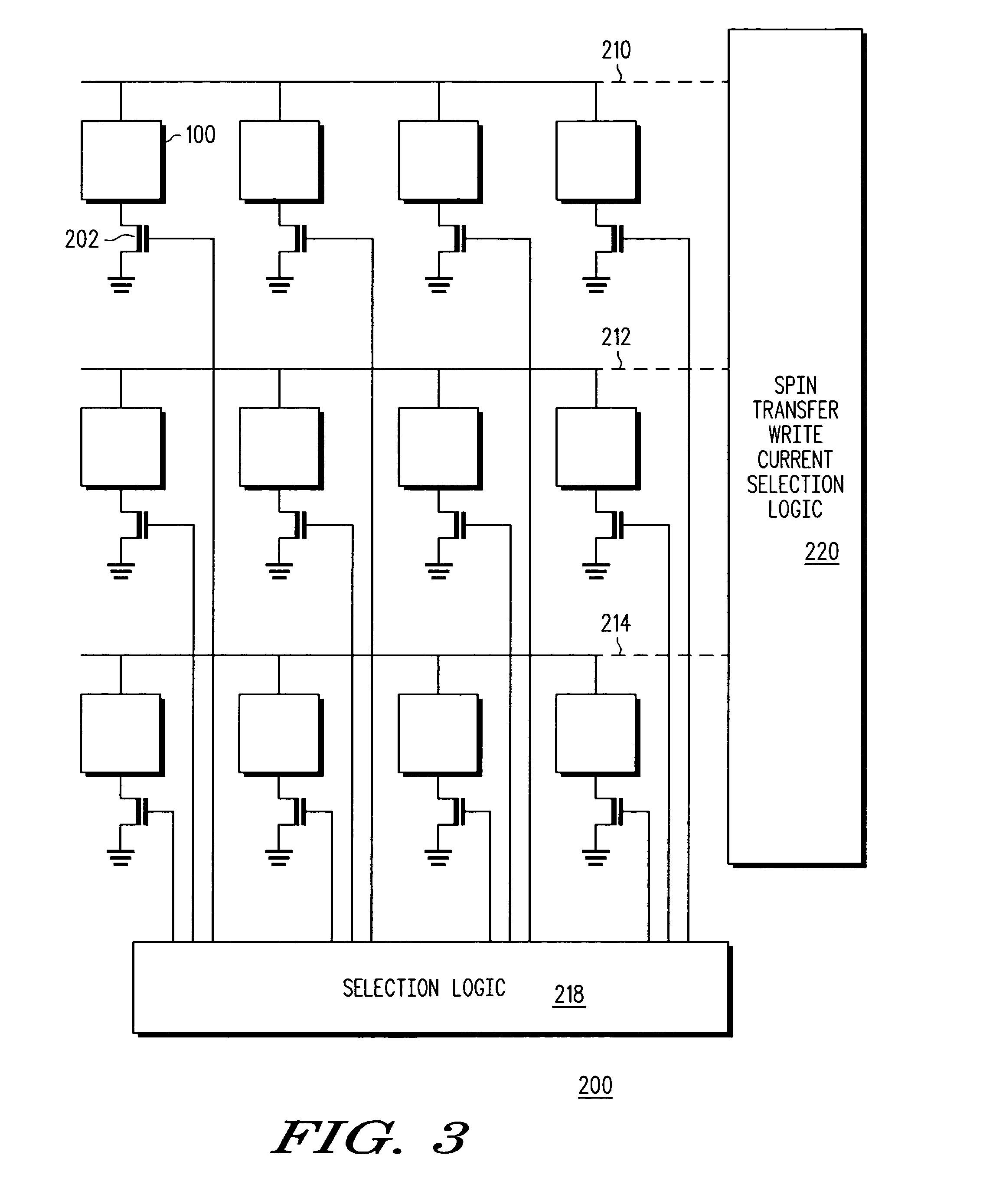
A magnetic random access memory device include a spin torque MRAM cell (100) having a reduced switching current (Ic) wherein standard materials may be used for a free layer (108). A fixed magnetic element (112) polarizes electrons passing therethrough, and the free magnetic element (108) having a first plane anisotropy comprises a first magnetization (130) whose direction is varied by the spin torque of the polarized electrons. An insulator (110) is positioned between the fixed magnetic element (112) and the free magnetic element (108), and a keeper layer (104) positioned contiguous to the free magnetic element (108) and having a second plane anisotropy orthogonal to the first plane anisotropy, reduces the first plane anisotropy and hence reduces the spin torque switching current (Ic). The keeper layer (104) may include alternating synthetic antiferromagnetic layers (132, 134) of magnetization approximately equal in magnitude and opposite in direction.

Description

FIELD OF THE INVENTION[0001]The present invention generally relates to magnetic random access memory (“MRAM”) devices, and more particularly relates to spin-transfer based MRAM devices.BACKGROUND OF THE INVENTION[0002]MRAM is a nonvolatile memory technology that uses magnetization to represent stored data, in contrast to older RAM technologies that use electronic charges to store data. One primary benefit of MRAM is that it retains the stored data in the absence of electricity, i.e., it is a nonvolatile memory. Generally, MRAM includes a large number of magnetic cells formed on a semiconductor substrate, where each cell represents one data bit. A bit is written to a cell by changing the magnetization direction of a magnetic element within the cell, and a bit is read by measuring the resistance of the cell (low resistance typically represents a “0” bit and high resistance typically represents a “1” bit).[0003]A practical MRAM device will typically include millions of cells. Generally...

Claims


Application Information

Patent Timeline
Patent Type & Authority Patents(United States)
IPC IPC(8): G11C11/14
CPCG11C11/16
Inventor RIZZO, NICHOLAS D.
Owner EVERSPIN TECHNOLOGIES
Learn More