Direct logical block addressing flash memory mass storage architecture

a mass storage and direct logical block technology, applied in the field of computers, can solve the problems affecting the performance of portable computers, etc., and achieve the effect of avoiding erasing cycles

Inactive Publication Date: 2009-04-21
MICRON TECH INC
View PDF345 Cites 40 Cited by
  • Summary
  • Abstract
  • Description
  • Claims
  • Application Information

AI Technical Summary

Benefits of technology

[0024]The device includes circuitry for performing two primary algorithms and an associated hardware architecture for a semiconductor mass storage device. The˜˜ first algorithm provides a means for mapping of host logical block address to physical block address with much improved performance and minimal hardware assists. In addition, the second algorithm provides means for avoiding an erase-before-write cycle when writing a modified data file back onto the mass storage device. Instead, no era-se is performed and the modified data file is written onto an empty portion of the mass storage.
[0026]According to the second algorithm, erase cycles are avoided by programming an altered data file into an empty mass storage block rather than itself after an erase cycle of the block as done on previous arts.

Problems solved by technology

Though widely used and commonly accepted, such hard disk drives suffer from a variety of deficiencies.
Because of the rotation of the disk, there is an inherent latency in extracting information from a hard disk drive.
Other problems are especially dramatic in portable computers.
Tin particular, hard disks are unable to withstand many of the kinds of physical shock that a portable computer will likely sustain.
Further, the motor for rotating the disk consumes significant amounts of power decreasing the battery life for portable computers.
Eventually, the dielectric deteriorates.
This process would have a major deterioration on overall system throughput.
This method has many deficiencies.
First, it introduces a delay in performance due to the erase operation before reprogramming the altered information.
In solid state flash, erase is a very slow process.
Secondly, hard disk users typically store two types of information, one is rarely modified and another which is frequently changed.
While this disparity has no impact on a hard disk because of its insensitivity to data changes, in a FLASH memory device, this variance can cause sections of the mass storage to wear out and be unusable significantly sooner than other sections of the mass storage.
This would ordinarily not be possible when using conventional mass storage because the central processor and commercial software available in conventional computer systems are not configured to track continually changing physical locations of data files.
Unfortunately, as is well known, CAM cells require multiple transistors, typically six.
Accordingly, the performance offered by this solution suffers because potentially all of the memory locations must be searched and compared to the desired logical block address before the physical location of the desired information can be determined.

Method used


Image

  • Direct logical block addressing flash memory mass storage architecture
  • Direct logical block addressing flash memory mass storage architecture
  • Direct logical block addressing flash memory mass storage architecture

Examples


Embodiment Construction

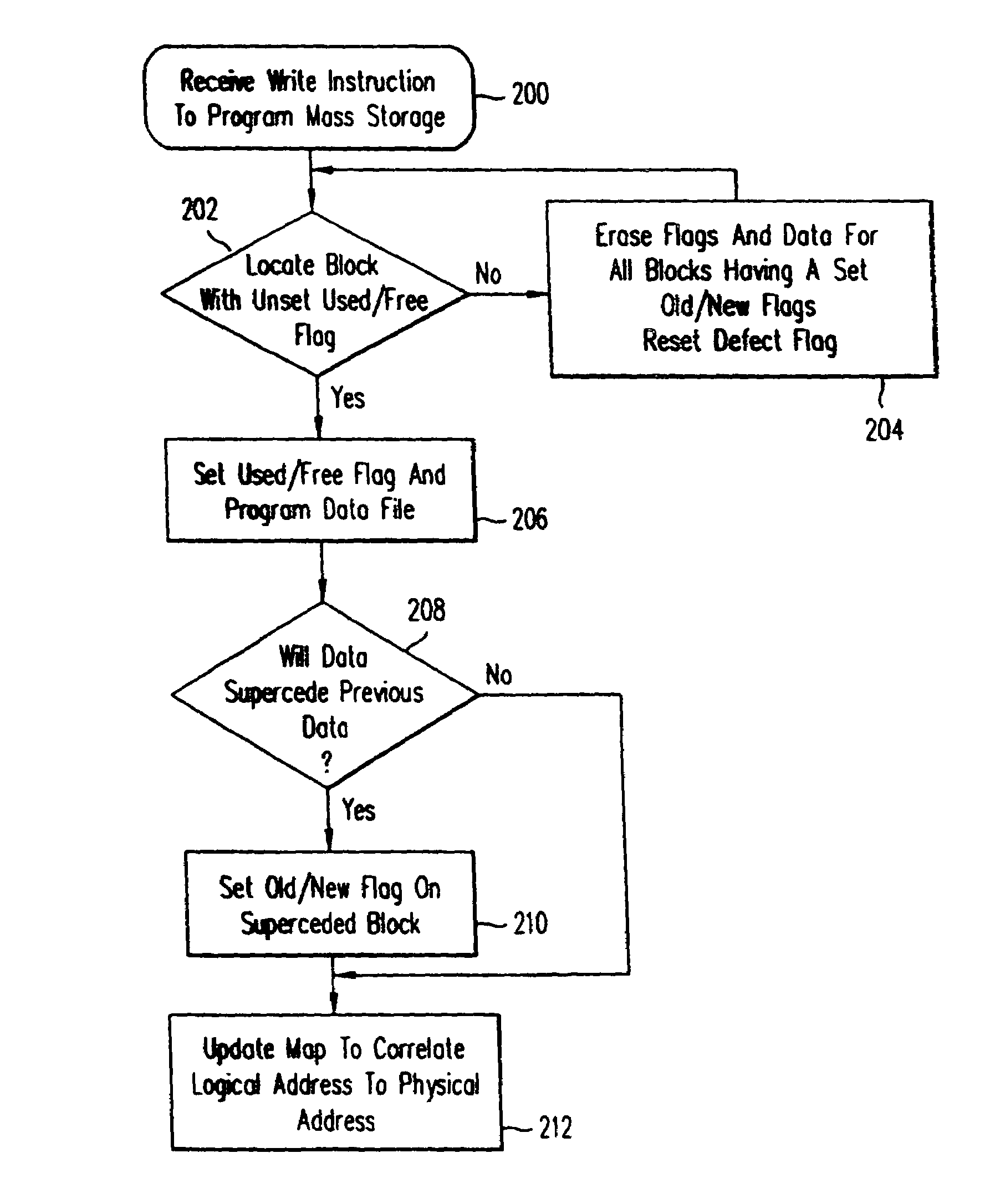
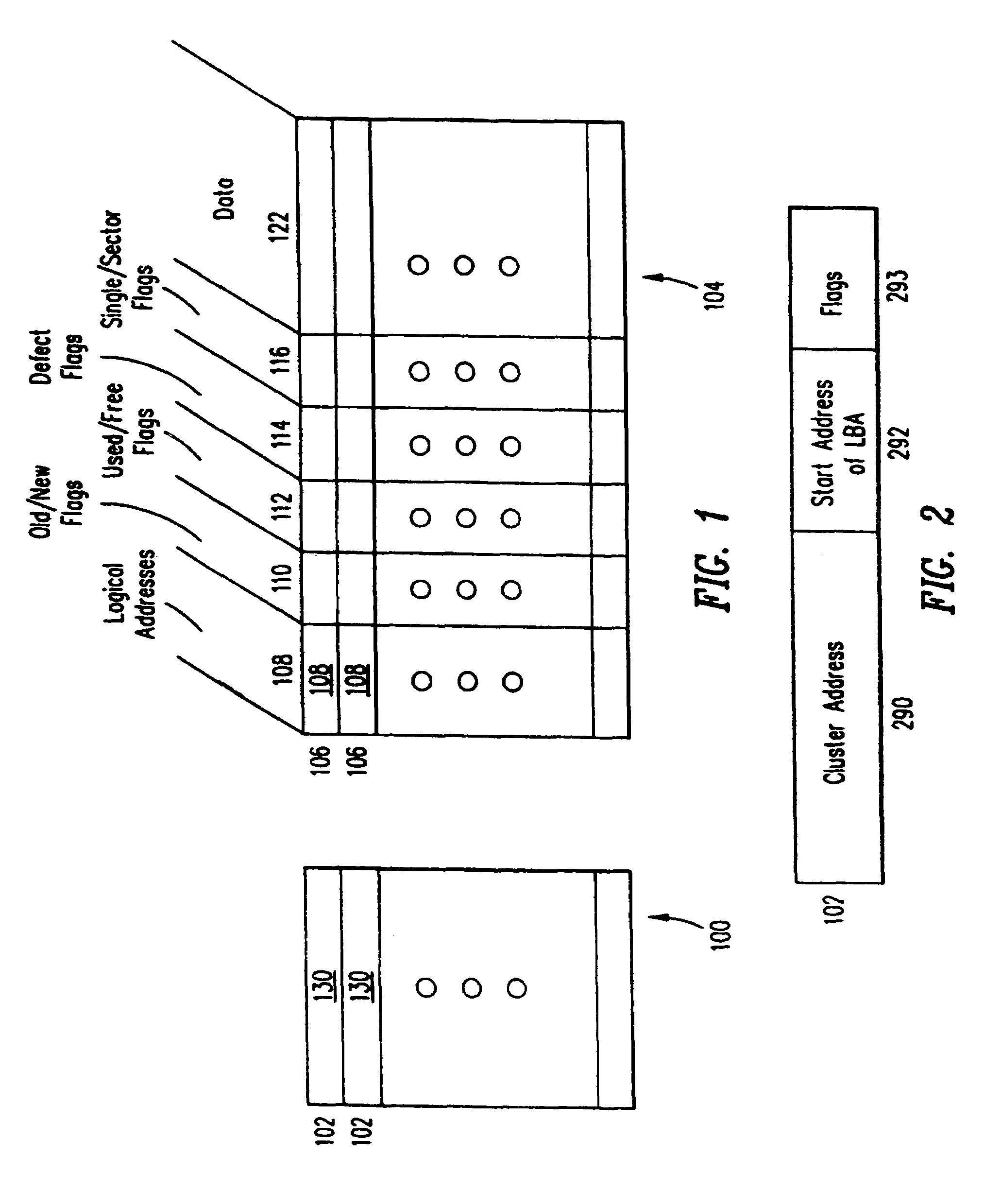
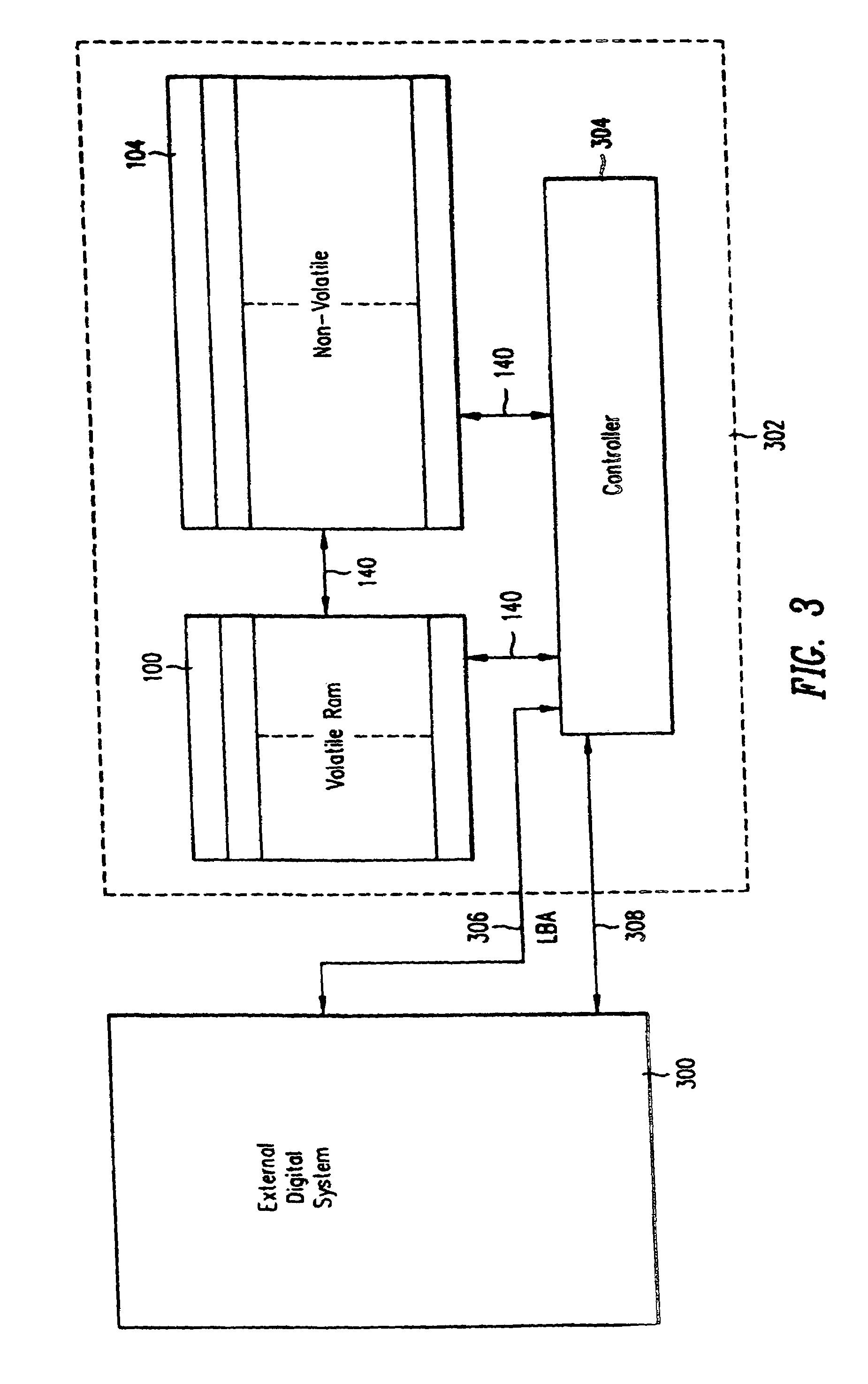
[0032]FIG. 1 shows an architecture for implementation of a solid state storage media according to the present invention. The storage media is for use with a host or other external digital system. The mass storage is partitioned into two portions, a volatile RAM array 100 and a nonvolatile array 104. According to the preferred embodiment, all of the nonvolatile memory storage is FLASH. The FLASH may be replaced by EEPROM. The RAM can be of any convenient type.

[0033]The memory storage 104 is arranged into N blocks of data from zero through N−1. Each of the blocks of data is M Bytes long. In the preferred embodiment, each data block is 512 Bytes long to correspond with a sector length in a commercially available hard disk drive plus the extra numbers of bytes to store the flags and logical block address information and the associated ECC. The memory 104 can contain as much memory storage as a user desires. An example of a mass storage device might include 100 M Byte of addressable stor...


PUM


Abstract

A nonvolatile semiconductor mass storage system and architecture can be substituted for a rotating hard disk. The system and architecture avoid an erase cycle each time information stored in the mass storage is changed. Erase cycles are avoided by programming an altered data file into an empty mass storage block rather than over itself as a hard disk would. Periodically, the mass storage will need to be cleaned up. These advantages are achieved through the use of several flags, and a map to correlate a logical block address of a block to a physical address of that block. In particular, flags are provided for defective blocks, used blocks, and old versions of a block. An array of volatile memory is addressable according to the logical address and stores the physical address.

Description

CROSS REFERENCE TO RELATED APPLICATIONS[0001]This application is a continuation of U.S. patent application Ser. No. 09 / 850,790, filed on May 7, 2001, now U.S. Pat. No. 6,912,618, issued on Jun. 28, 2005, and entitled“DIRECT LOGICAL BLOCK ADDRESSING FLASH MEMORY MASS STORAGE ARCHITECTURE.,” which is a continuation of U.S. application Ser. No. 09 / 521,420, filed Mar. 8, 2000, now U.S. Pat. No. 6,230,234, issued on May 8, 2001 and entitled “DIRECT LOGICAL BLOCK ADDRESSING FLASH MEMORY MASS STORAGE ARCHITECTURE.,” which is a continuation of U.S. application Ser. No. 09 / 311,045, filed May 13, 1999, now U.S. Pat. No. 6,115,785, issued on Sep. 5, 2000 and entitled “DIRECT LOGICAL BLOCK ADDRESSING FLASH MEMORY MASS STORAGE ARCHITECTURE.” which is a continuation of U.S. application Ser. No. 09 / 087,720, filed May 29, 1998, now U.S. Pat. No. 5,924,113 issued on Jul. 13, 1999, entitled “DIRECT LOGICAL BLOCK ADDRESSING FLASH MEMORY MASS STORAGE ARCHITECTURE.” which is a continuation of U.S. appli...

Claims


Application Information

Patent Timeline
Patent Type & Authority Patents(United States)
IPC IPC(8): G06F12/10G06F3/06G06F11/10G06F12/02G11C16/08G11C16/10G11C29/00
CPCG06F3/0613G06F3/0616G06F3/064G06F3/0679G06F12/023G06F12/0246G11C16/08G11C16/102G11C29/765G11C29/82G06F11/1068
Inventor ESTAKHRI, PETROASSAR, MAHMUD
Owner MICRON TECH INC
Why Eureka
Try Eureka