
Electron emitter and method of fabricating electron emitter

a technology of electron emitter and electron emitter, which is applied in the manufacture of electrode systems, electric discharge tube/lamps, and discharge tube luminescnet screens, etc. it can solve the problems of complex fabrication process, increased component costs, and high fabrication costs of apparatus, and achieves enhanced electron emission quantity, increased electric field concentration, and easy excitation high electric field concentration

Inactive Publication Date: 2009-05-05
NGK INSULATORS LTD
View PDF37 Cites 4 Cited by
  • Summary
  • Abstract
  • Description
  • Claims
  • Application Information

AI Technical Summary

Benefits of technology

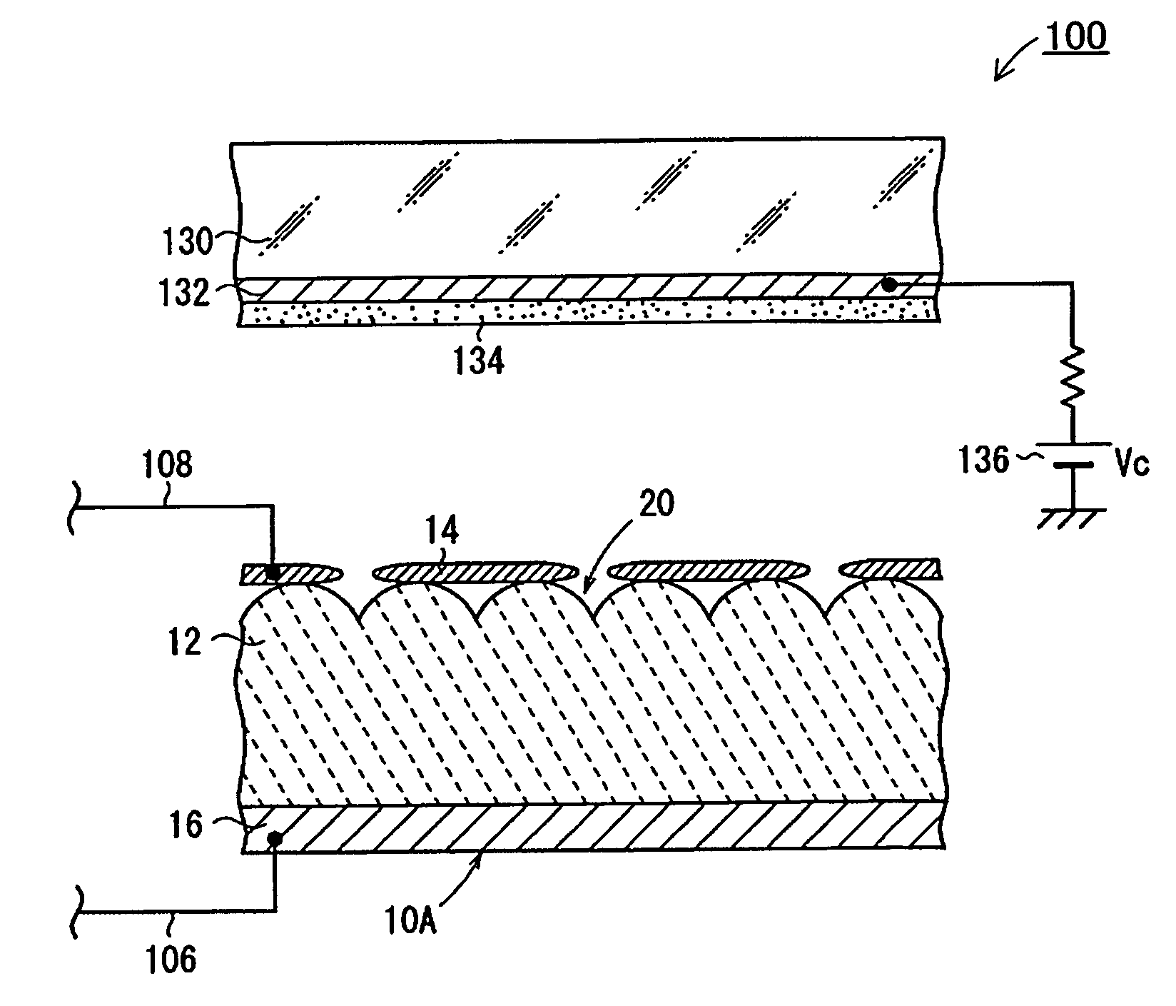
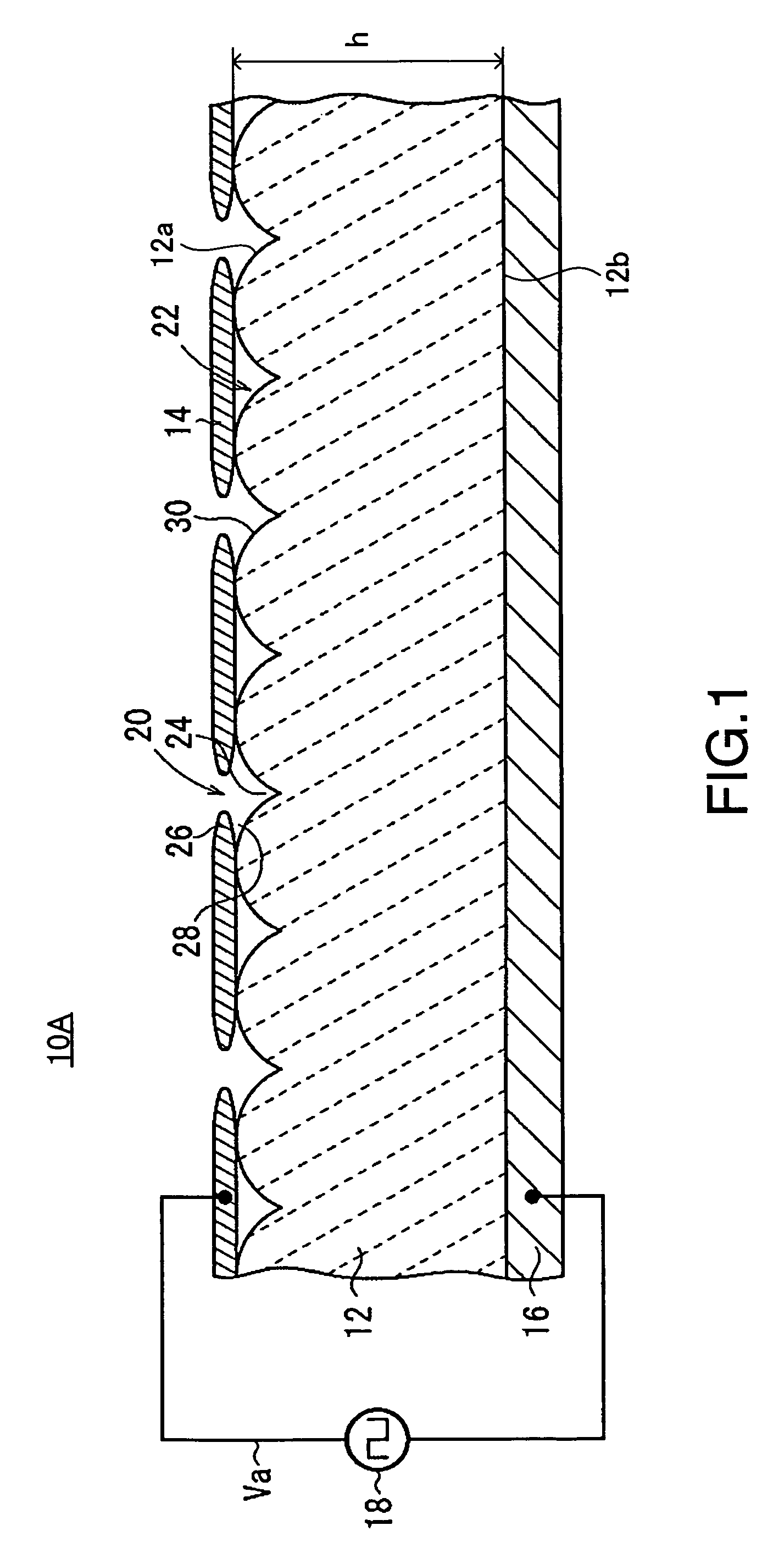
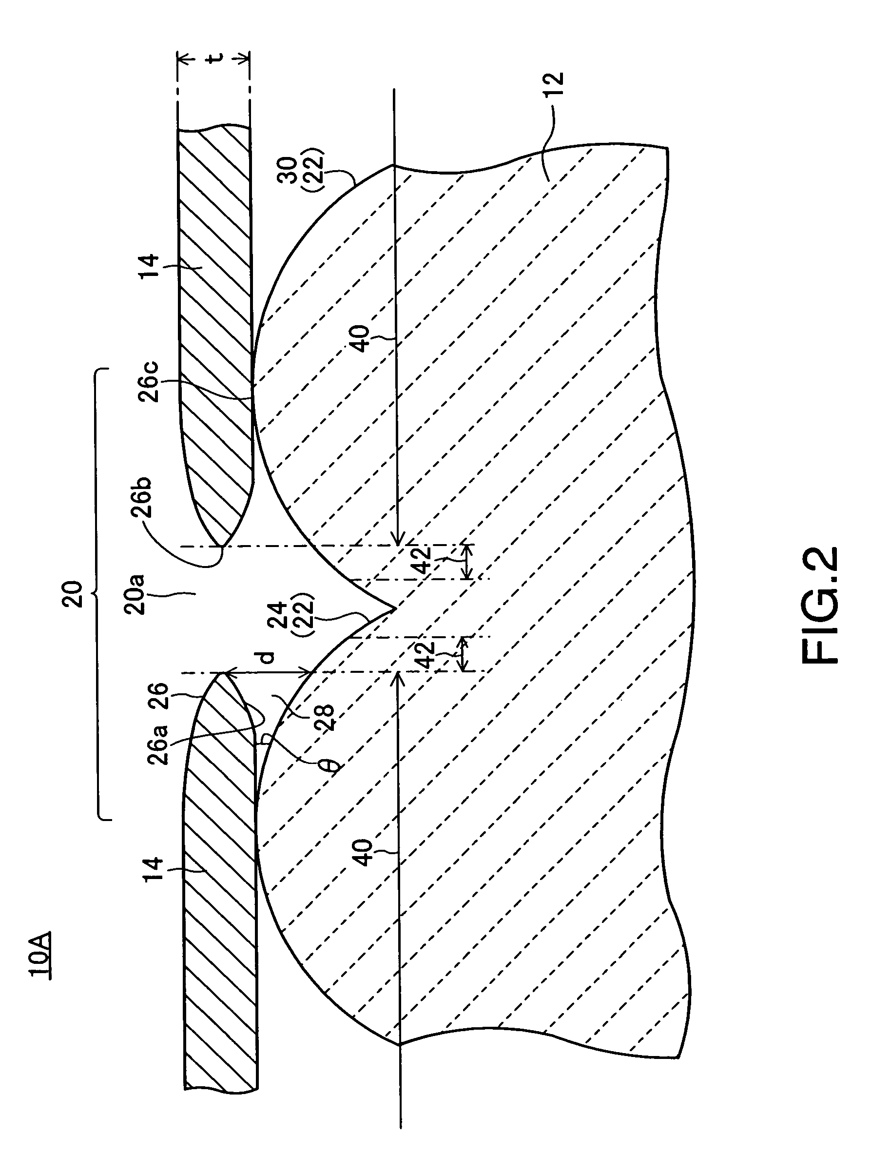
[0017]According to the above-mentioned configuration of the present invention, the opening portion of the first electrode is apart from the first surface of the emitter layer, whereby a gap is formed between the first surface and a surface of the opening portion of the first electrode facing the first surface, and the cross section of the opening portion of the first electrode assumes the form of an overhanging portion (flange). Additionally, the opening portion has a shape which causes lines of electric force to concentrate at the inner edge thereof. Accordingly, in the opening portion, a triple junction, which serves as an electric field concentration point, arises at a position different from the inner edge of the opening portion, and an electric field concentration point also arises on the inner edge of the opening portion. Thus, the number of electron-emitting sites can be increased.
[0039]As described above, the electron emitter according to the present invention can readily excite high electric field concentration and can increase the number of electric field concentration points. Therefore, the present invention can provide an electron emitter having enhanced electron emission quantity.

Problems solved by technology

Since micromachining that involves etching, forming, or the like is required for forming such fine conductive electrodes, a fabrication process becomes complicated.
Since high voltage must be applied for emitting electrons, ICs for high-voltage drive and like components must be used, resulting in increased component costs.
Thus, the disclosed electron emitters involve a problem of high fabrication costs and an associated increase in fabrication costs for apparatus to which the electron emitters are applied.
Thus, the number of electron-emitting sites is limited.

Method used


Image

  • Electron emitter and method of fabricating electron emitter
  • Electron emitter and method of fabricating electron emitter
  • Electron emitter and method of fabricating electron emitter

Examples


example 1

[0140]10 percent by weight scale-like graphite powder (trade name “SP20” (average particle size 15 μm, thickness about 2 μm), product of Nippon Graphite Industry Co., LTD.), 1 percent by weight dispersant (trade name “Disperbyk-108,” product of BYK-Chemie, Germany), and 25 percent by weight binder (a mixture of ethyl cellulose and 2-ethylhexanol mixed at a ratio of 25:75) were mixed by use of the tri roll mill. When the graphite powder is aggregated, the graphite powder needs to be pretreated; specifically, grounded by use of a homogenizer.

[0141]Next, Ag resinate (trade name “XE109-4,” product of Namics Corporation) was added to the above-prepared mixture such that the ratio by volume between graphite and silver becomes 9:1. The resultant mixture was mixed by use of the tri roll mill, thereby yielding a paste.

[0142]The thus-obtained paste was diluted with terpineol to a viscosity of about in the range from 100,000 cp to 200,000 cp. The thus-prepared paste was applied to the dielectr...

example 2

[0143]The electrode was formed in a manner similar to that of Example 1 except that scale-like graphite powder (trade name “KS25” (average particle size 25 μm, thickness about 2 μm), product of TIMCAL Ltd.) and Ag ink were used. The Ag ink was composed of a dispersion medium and silver fine particles, which were dispersed in the dispersion medium, and prepared by mixing 5 percent by weight NPS-J (trade name, product (average particle size: about 7 nm) of Harima Chemicals, Inc.), 10 percent by weight low-polymerization-degree polyvinyl butyral (trade name “S-LEC B BL-S,” product of Sekisui Chemical Co., Ltd.), and 10 percent by weight terpineol. The mixing ratio was similar to that of Example 1. As in the case of Example 1, formation of opening portions each having an opening of several μm to 10 μm in size was confirmed.

[0144]The electron emitter according to the present invention is not limited to the above embodiments, but may assume various other configurations so long as the esse...


PUM


Abstract

An electron emitter includes an emitter layer formed of a dielectric material, an upper electrode, and a lower electrode. A drive voltage is applied between the upper electrode and the lower electrode, for emitting electrons. The upper electrode is formed of scale-like conductive particles on the upper surface of the emitter layer and has a plurality of opening portions. The surfaces of overhanging portions of the opening portions that face the emitter layer are apart from the emitter layer. The overhanging portions each have such a cross-sectional shape as to be acutely pointed toward the inner edge of the opening portion, or the tip end of the overhanging portion, so that lines of electric force concentrate at the inner edge.

Description

CROSS REFERENCE TO RELATED APPLICATIONS[0001]This application is a continuation-in-part of U.S. Application Ser. No. 10 / 877,517, filed Jun. 25, 2004 now abandoned, and also claims the benefit under 35 USC § 119(e) of U.S. Provisional Application Serial No. 60 / 640,169, filed Dec. 27, 2004, the entireties of which are incorporated herein by reference.[0002]This application claims the benefit of Japanese Application No. 2004 -169997, filed Jun. 8, 2004, and Japanese Application No. 2004-194472, filed Jun. 30, 2004, the entireties of which are incorporated herein by reference.BACKGROUND OF THE INVENTION[0003]1. Field of the Invention[0004]The present invention relates to an electron emitter applicable to electron beam sources for use in various devices and apparatus that utilize electron beam, such as field emission displays (FEDs), backlight units, electron beam irradiation apparatus, light sources, electronic parts manufacturing apparatus, and electronic circuit components, as well as...

Claims


Application Information

Patent Timeline
Patent Type & Authority Patents(United States)
IPC IPC(8): H01J1/46H01J1/00H01J1/02H01J1/14H01J1/312H01J1/32H01J9/02
CPCB82Y10/00H01J1/312H01J1/32H01J9/022
Inventor OHWADA, IWAOSATO, KEIKOBAYASHI, NOBUYUKIYOKOYAMA, SHOHEI
Owner NGK INSULATORS LTD
Learn More