Piezoelectric element, inkjet head, angular velocity sensor, methods for manufacturing them and inkjet recording device

a technology of piezoelectric element and angular velocity sensor, which is applied in the direction of device material selection, distance measurement, instruments, etc., can solve the disadvantageous limitation of monocrystalline mgo substrate material, high piezoelectric displacement property, and high durability

Active Publication Date: 2009-05-12
PANASONIC CORP
View PDF24 Cites 6 Cited by
  • Summary
  • Abstract
  • Description
  • Claims
  • Application Information

AI Technical Summary

Benefits of technology

[0151]The piezoelectric element according to the present invention achieves high piezoelectric displacement property and high durability.
[0152]The method for manufacturing the piezoelectric element according to the present invention makes it possible to easily mass-produce the piezoelectric element having high piezoelectric displacement property and high durability. Therefore, even through mass production, piezoelectric elements having excellent resistance to voltage and durability are obtained with excellent repeatability of the piezoelectric property and less variations in piezoelectric property.
[0153]The inkjet head and the inkjet recording device according to the present invention reduce variations in ink discharge performance and achieve high durability.
[0154]The angular velocity sensor according to the present invention achieves downsizing and high dimensional precision. Even if the angular velocity sensor is put into mass production, angular velocity sensors having excellent resistance to voltage and durability are achieved with excellent repeatability of the property and less variations in property.

Problems solved by technology

In this case, however, since the monocrystalline MgO substrate is used as a base substrate, the obtained piezoelectric element will be expensive and an inkjet head using the piezoelectric element will also be expensive.
Moreover, the substrate material is disadvantageously limited to monocrystalline MgO only.
However, unlike the method of forming the thin piezoelectric film on the monocrystalline MgO substrate, it is difficult to obtain a thin, highly crystalline piezoelectric film having crystal orientation defined at the time when the film has been formed because the sol-gel method is used.
If mass production of the piezoelectric element is carried out by the sol-gel method, a thin amorphous precursor film of the thin piezoelectric film is likely to cause cracks due to a change in volume in a degreasing step for removing organic matters.
Further, in the step of heating the thin amorphous precursor film of the thin piezoelectric film at a high temperature for crystallization, cracks are easily generated due to a change in crystallinity and the film is likely to fall off the bottom electrode.
Therefore, in order to achieve a thickness of 1 μm or more required for achieving the piezoelectric element, the step needs to be carried out 10 or more times. This brings about a problem of reduction of yield.
Therefore, like the sol-gel method, cracks are easily generated or the film is likely to fall off the bottom electrode due to a change in crystallinity in the high-temperature heating step for crystallization.
However, the orientation film has not been achieved by the other methods than the sol-gel method.
Therefore, the crystallization is hard to control in these methods.

Method used


Image

  • Piezoelectric element, inkjet head, angular velocity sensor, methods for manufacturing them and inkjet recording device
  • Piezoelectric element, inkjet head, angular velocity sensor, methods for manufacturing them and inkjet recording device
  • Piezoelectric element, inkjet head, angular velocity sensor, methods for manufacturing them and inkjet recording device

Examples


embodiment 1

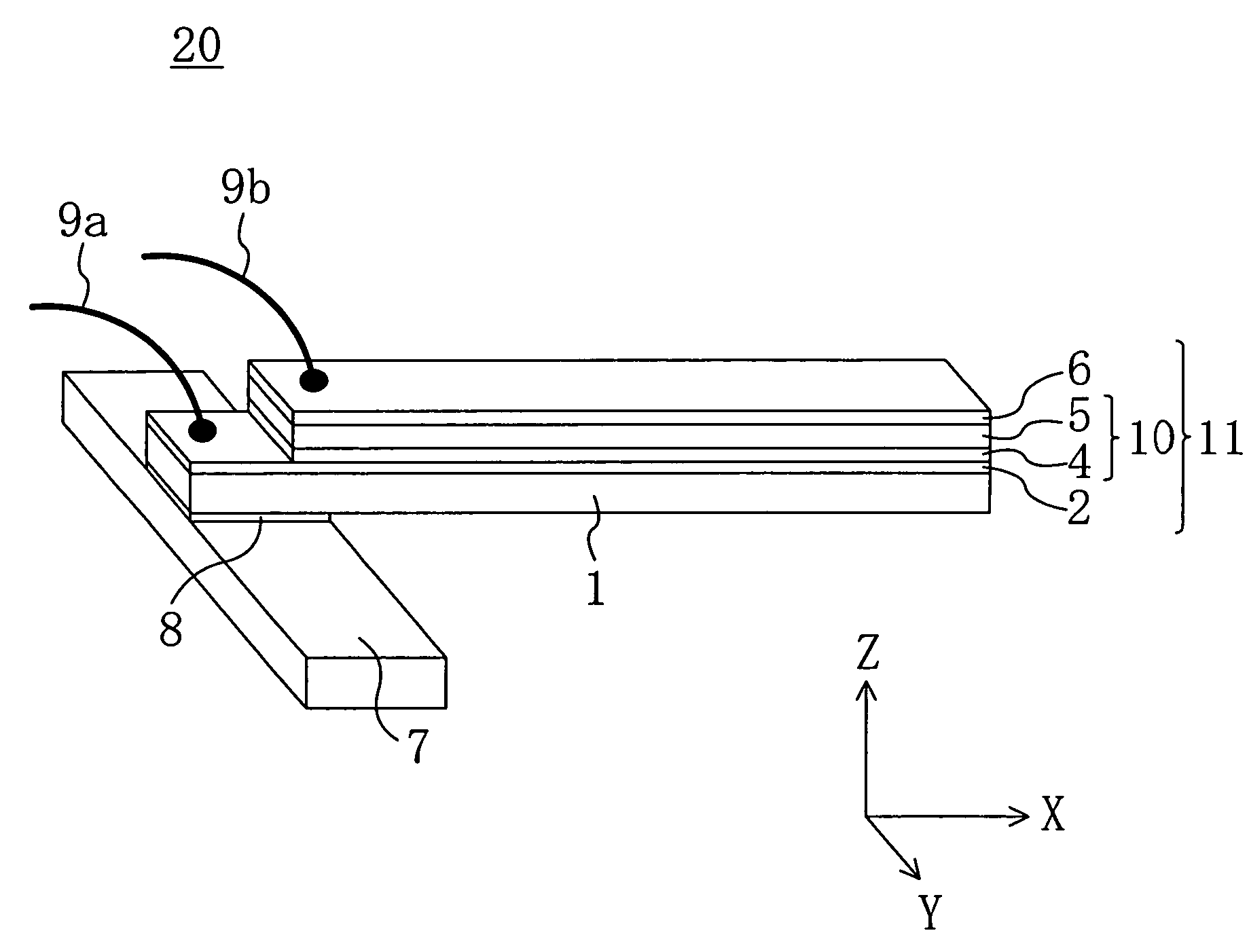
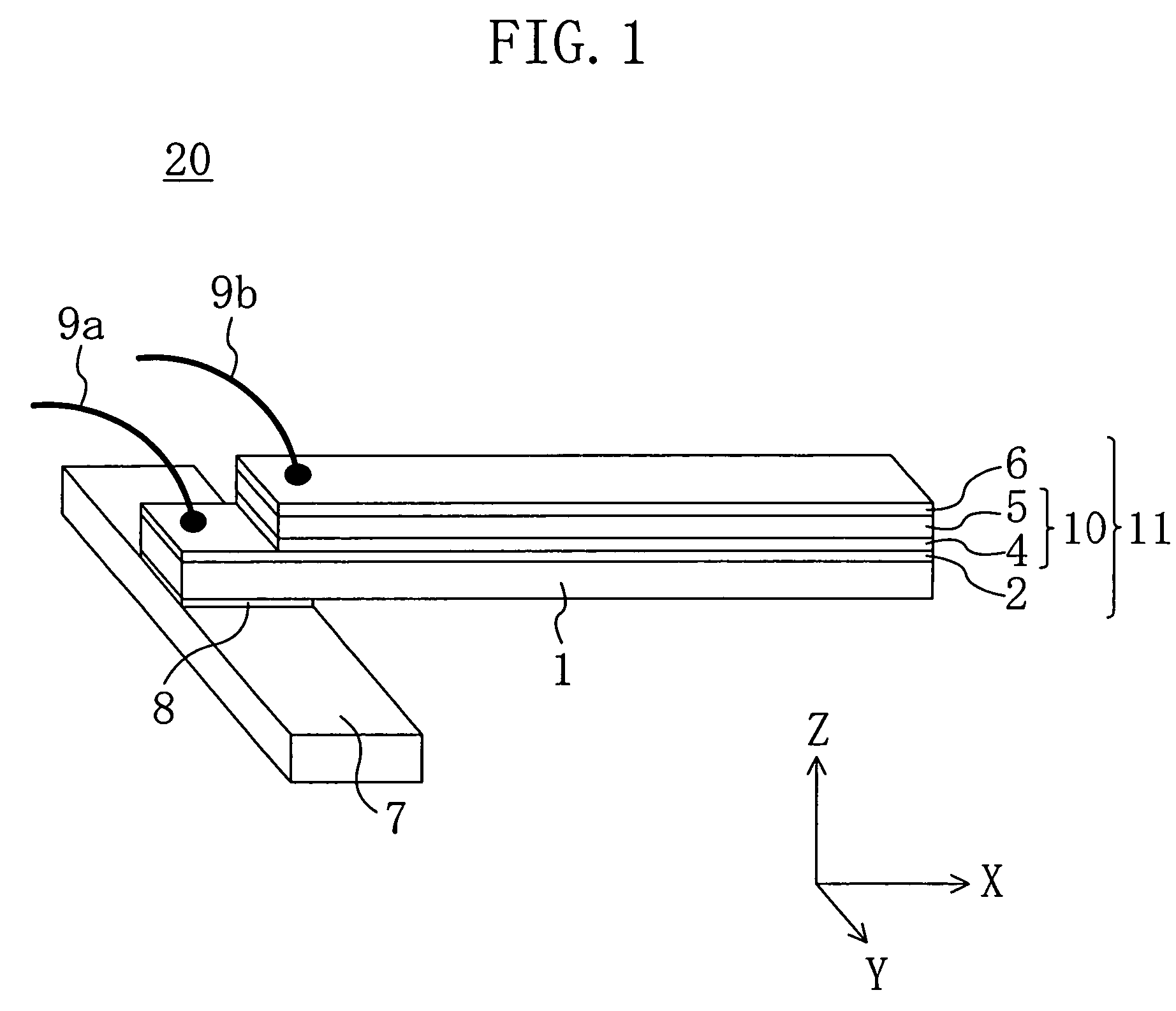
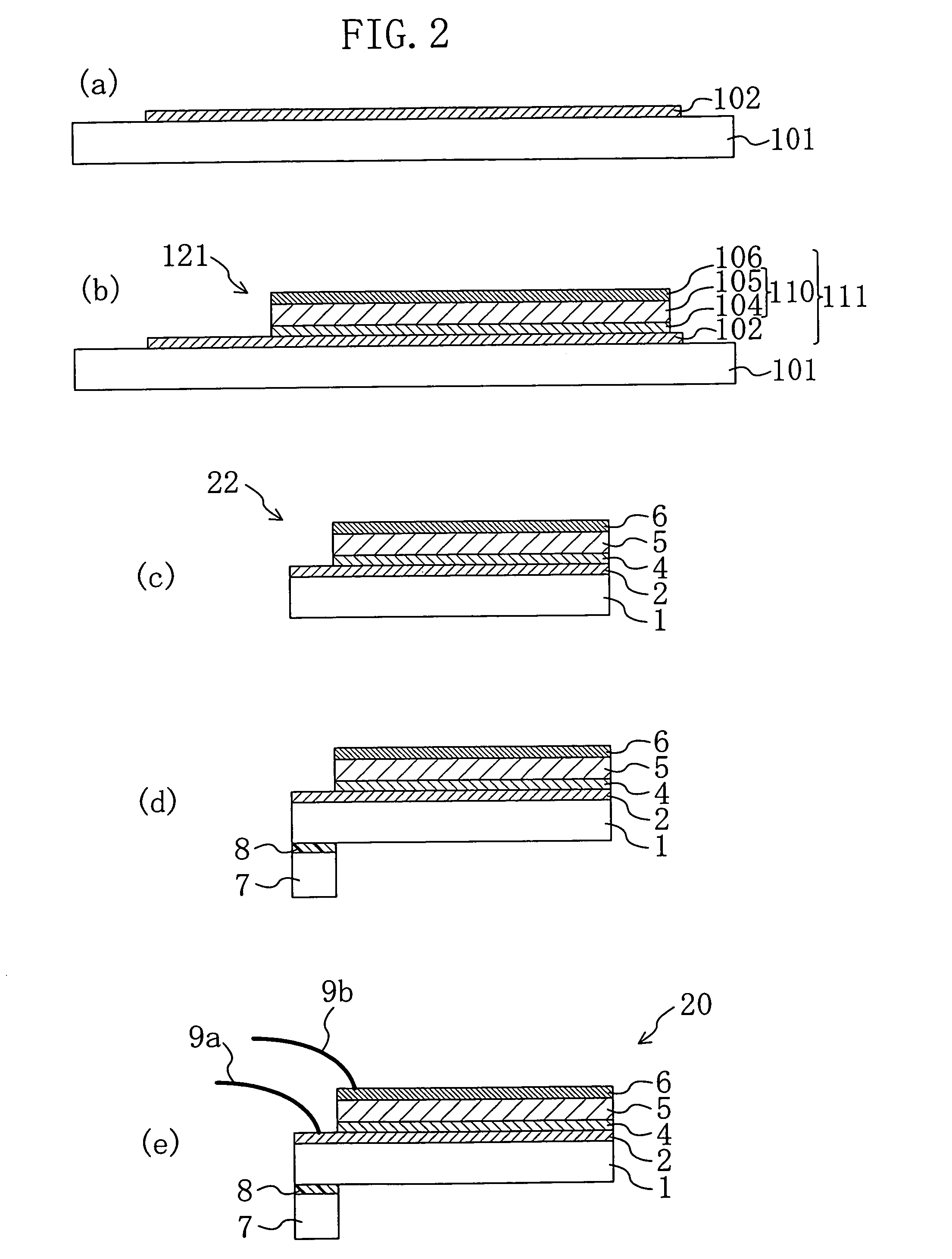
[0189]FIG. 1 is an oblique view illustrating a piezoelectric element 20 according to Embodiment 1 of the present invention. As shown in FIG. 1, the piezoelectric element 20 includes a substrate 1 which is in the form of a flat strip of 15.0 mm in length, 0.40 mm in thickness and 3.0 mm in width and a layered body 11 disposed on the substrate 1. The substrate 1 functions as a diaphragm which hinders expansion and contraction of the layered body 11 caused by the piezoelectric effect. The piezoelectric element 20 is 3.0 mm in width. An end portion of the piezoelectric element 20 having a width of 3.0 mm and a length of 3.0 mm (a left end portion in FIG. 1) is fixed onto a 1.0 mm thick support substrate 7 made of stainless steel (3.0 mm in width and 10.0 mm in length) with an epoxy-based adhesive 8. Thus, the piezoelectric element 20 is provided in the form of a cantilever.

[0190]A first electrode film 2 is provided on the substrate 1. On the surface of the first electrode film 2 except ...

example 1

[0206]Silicon was used as the substrate. A thin iridium (Ir) film having a thickness of 100 nm was used as the first electrode film. In order to form the thin iridium film, the substrate was preheated at 400° C. in a ternary RF magnetron sputtering apparatus. Then, sputtering was carried out using a gas mixture of argon and oxygen (gas volume ratio Ar:O2=15:1) as sputtering gas at a total gas pressure maintained at 0.25 Pa and a 4-inch diameter iridium target as a first target under a high frequency power of 200 W for 960 seconds.

[0207]A layered piezoelectric film was provided by forming a first thin piezoelectric film which is made of a 50 nm thick PZT film having (111) preferred orientation and a second thin piezoelectric film which is formed on the first piezoelectric film and made of a 3400 nm thick PZT film having (111) orientation. That is, the thickness of the layered piezoelectric film was 3450 nm.

[0208]The first and second thin piezoelectric films were formed using a RF mag...

example 2

[0218]High-temperature resistant Pyrex (registered trademark) glass was used as the substrate. A 150 nm thick platinum (Pt) film was used as the first electrode film. In order to form the thin platinum film, the substrate was preheated at 400° C. in a ternary RF magnetron sputtering apparatus. Then, sputtering was carried out using a gas mixture of argon and oxygen (gas volume ratio Ar:O2=15:1) as sputtering gas at a total gas pressure maintained at 0.25 Pa and a platinum target as a first target under a high frequency power of 200 W for 1080 seconds.

[0219]A layered piezoelectric film was provided by forming a first thin piezoelectric film made of a 100 nm thick PZT film having (111) preferred orientation and a second thin piezoelectric film made of a 4000 nm thick PZT film having (111) crystal orientation. That is, the thickness of the layered piezoelectric film was 4100 nm.

[0220]In the same manner as Example 1, the first and second thin piezoelectric films were formed using a RF m...


PUM


Abstract

A piezoelectric element includes two electrode films and a layered piezoelectric film which is sandwiched between the electrode films and made of two thin piezoelectric films each having preferred orientation along the (111) plane. The two thin piezoelectric films are aggregates of columnar grains, respectively, which are continuously linked to each other. The columnar grains of the second thin piezoelectric film have a larger average cross-sectional diameter than the columnar grains of the first thin piezoelectric film. The ratio of the thickness of the layered piezoelectric film to the average cross-sectional diameter of the columnar grains of the second thin piezoelectric film is 20 to 60 inclusive.

Description

TECHNICAL FIELD[0001]The present invention relates to a piezoelectric element which exhibits electromechanical transduction properties, an inkjet head and an angular velocity sensor using the piezoelectric element, methods for manufacturing them and an inkjet recording device using the inkjet head.BACKGROUND ART[0002]Piezoelectric material is material which converts mechanical or electrical energy to electrical or mechanical energy. A typical example of the piezoelectric material is an oxide having a perovskite crystal structure such as lead zirconate titanate (Pb(Zr, Ti)O3, hereinafter referred to as PZT). Regarding the ratio between Zr and Ti Zr / Ti=53 / 47 at % as a threshold, perovskite PZT becomes rhombohedral when the ratio of Zr is high, or tetragonal when the ratio of Zr is low. The rhombohedral PZT gives the maximum piezoelectric displacement along the (111) axis, while the tetragonal PZT gives the maximum piezoelectric displacement along the (001) axis (c-axis). However, most...

Claims


Application Information

Patent Timeline
Patent Type & Authority Patents(United States)
IPC IPC(8): B41J2/045B41J2/055B41J2/135B41J2/14B41J2/16G01C3/08G01C19/56G01C19/5621G01C19/5628H01L41/08H01L41/09H01L41/18H01L41/187H01L41/22H01L41/29H01L41/316H01L41/319H01L41/332
CPCB41J2/14233B41J2/161B41J2/1623B41J2/1628B41J2/1629B41J2/1631B41J2/1646G01C19/5628H01L41/316H01L41/0815H01L41/094H01L41/0973H01L41/1876B41J2002/1425B41J2002/14258H10N30/10516H10N30/2042H10N30/2047H10N30/8554H10N30/076
Inventor TOMOZAWA, ATSUSHIFUJII, EIJITORII, HIDEO
Owner PANASONIC CORP
Why Eureka
Try Eureka