Method of fabricating sample membranes for transmission electron microscopy analysis

a technology of transmission electron microscopy and sample lamella, which is applied in the direction of material analysis using wave/particle radiation, instruments, nuclear engineering, etc., can solve the problems of affecting the analysis of defects, the chip structure is not good, and the resolution is relatively weak for high-density devices, etc., to achieve the effect of easy fabrication of sample lamella

a technology of transmission electron microscopy and sample lamella, which is applied in the direction of material analysis using wave/particle radiation, instruments, nuclear engineering, etc., can solve the problems of affecting the analysis of defects, the chip structure is not good, and the resolution is relatively weak for high-density devices, etc., to achieve the effect of easy fabrication of sample lamella

US7538322B2Active Publication Date: 2009-05-26MICRON TECH INC

Image

  • Method of fabricating sample membranes for transmission electron microscopy analysis
  • Method of fabricating sample membranes for transmission electron microscopy analysis
  • Method of fabricating sample membranes for transmission electron microscopy analysis

Examples


Embodiment Construction

[0022]The accompanying drawings are included to provide a further understanding of the invention, and are incorporated in and constitute a part of this specification. The drawings illustrate embodiments of the invention and, together with the description, serve to explain the principles of the invention.

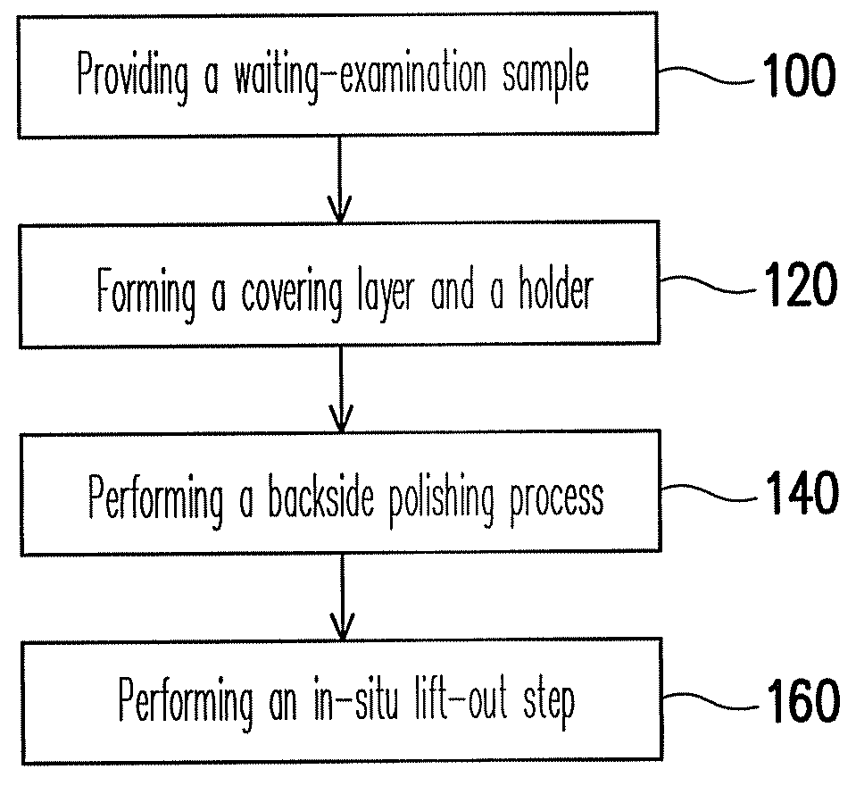
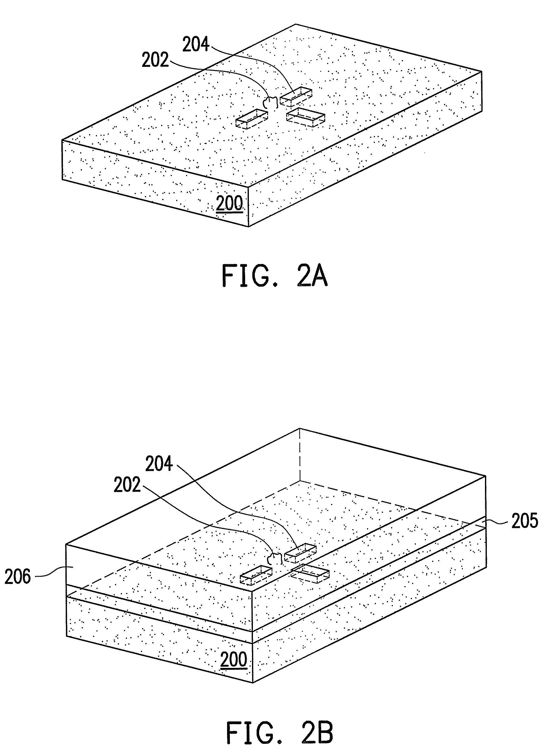
[0023]FIG. 1 is a flow chart showing the steps of the method of fabricating sample membrane for TEM analysis according to an embodiment of the present invention. FIGS. 2A to 2D are schematic sectional views of the process steps of the method of fabricating sample membrane for TEM analysis according to an embodiment of the present invention.

[0024]First, referring to FIGS. 1 and 2A together, the method of fabricating the sample lamella for TEM analysis comprises the following steps. First, a waiting-examination sample 200 is provided (step 100). The waiting-examination sample 200 comprises, for example, a small portion of a wafer. Generally speaking, devices such as memories and metal ...


PUM

PropertyMeasurementUnit
thicknessaaaaaaaaaa
depthaaaaaaaaaa
lengthaaaaaaaaaa

Abstract

A method of fabricating sample lamella for transmission electron microscopy (TEM) analysis is provided. A waiting-examination sample having an analysis target on the top surface of that is offered, and at least a mark around the analysis target is defined. A covering layer is covered on the top surface of waiting-examination sample. A holder is attached on the covering layer. A backside polishing process is performed to remove a portion of the waiting-examination sample until the mark is visible under the optical microscopy from the bottom surface of waiting-examination sample. An in-situ lift-out step is performed to pick up a thin membrane containing the analysis target and serve as the sample for TEM analysis.

Description

CROSS-REFERENCE TO RELATED APPLICATION[0001]This application claims the priority benefit of Taiwan application serial no. 95132838, filed Sep. 6, 2006. All disclosure of the Taiwan application is incorporated herein by reference.BACKGROUND OF THE INVENTION[0002]1. Field of the Invention[0003]The present invention relates to a semiconductor measurement and analysis technology. More particularly, the present invention relates to a method of fabricating sample lamella for transmission electron microscopy (TEM) analysis.[0004]2. Description of Related Art[0005]During the failure analysis and the process evaluation of VLSI (very large scale integration) device, cross-section analysis is considered as an effective technology. The scanning electron microscopy (SEM) is a tool for observing the cross-section, but the resolution is relatively weak for the high-density device. Therefore, when the semiconductor process progresses into the stage of VLSI, SEM are gradually replaced by TEMs. The T...

Claims


Application Information

Patent Timeline
26 May 2009
Publication
US7538322B2
IPC
G01N1/28; G01N23/04
CPC
G01N1/2813; G01N23/225
Inventors
LUO, JIAN-SHING; HUANG, LANG-YU