
Design for a field emission display with cathode and focus electrodes on a same level

a field emission display and focus electrode technology, applied in the field of field emission display, can solve the problems of inability to produce separate layers and drawbacks of adding process steps, and achieve the effects of simple structure, enhanced electron beam focusing characteristics, and easy manufacturing

Inactive Publication Date: 2009-06-09
SAMSUNG SDI CO LTD
View PDF11 Cites 4 Cited by
  • Summary
  • Abstract
  • Description
  • Claims
  • Application Information

AI Technical Summary

Benefits of technology

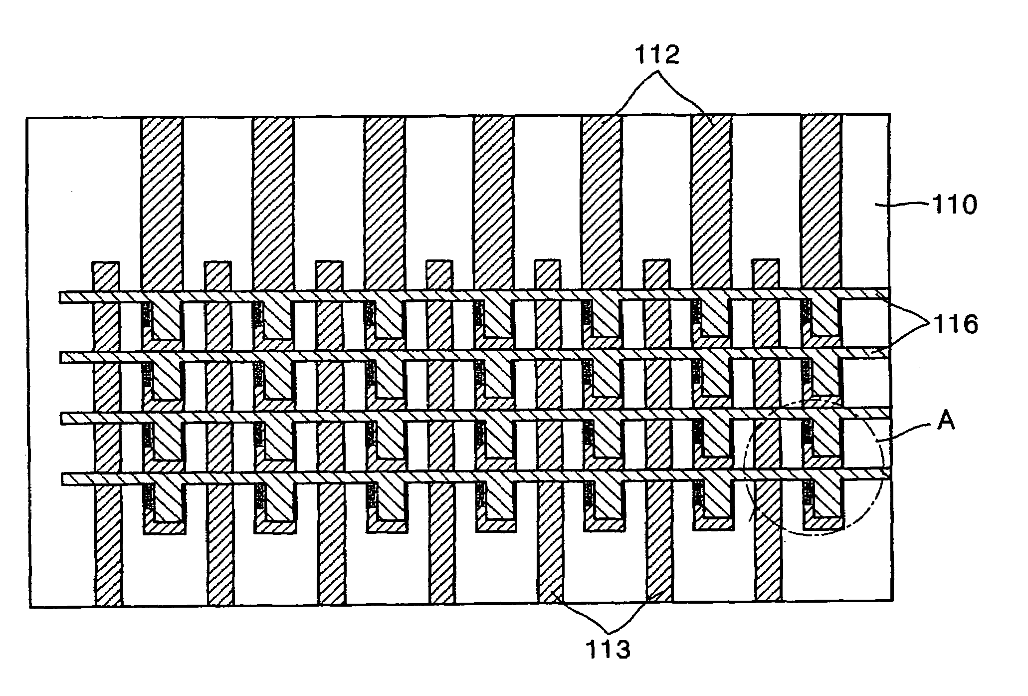
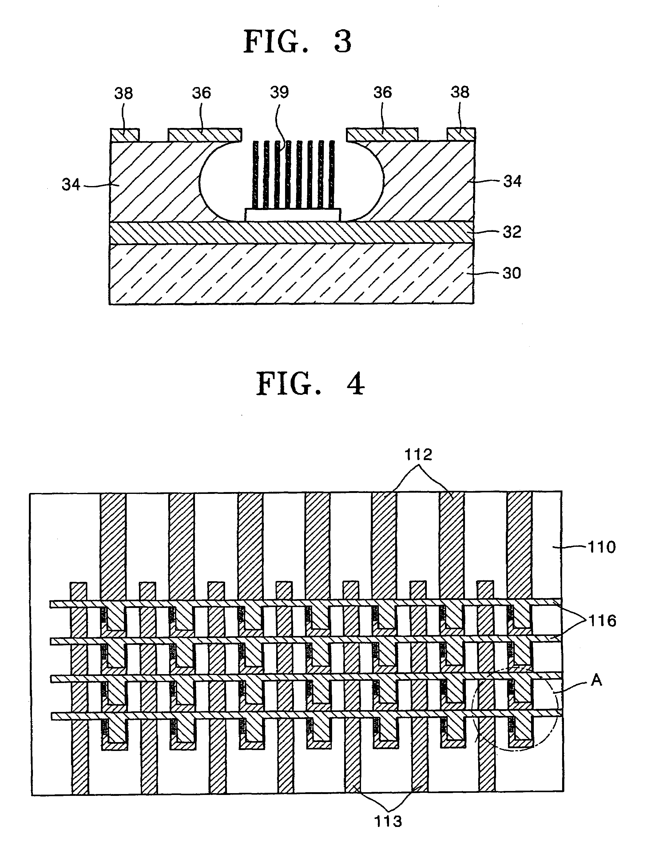
The present invention provides an improved design for an FED that properly focuses electron beams without excess process steps. The FED has a simple structure that is easy to manufacture and includes a cathode electrode and a focus electrode on the same level with each other on the substrate. The FED has enhanced focusing characteristics of electron beams and a field emitter formed at the cathode electrode. The field emitter may be formed of carbon nanotubes, graphite nanoparticles, nano diamond, boron nitride, diamond-like carbon, iron, nickel, copper, or magnesium oxide. The method of manufacturing the FED involves coating electrode material on a substrate, patterning the electrode material, forming an insulation layer, and forming a gate electrode. The field emitter may be formed at an exposed portion of the cathode electrode that faces the focus electrode. The invention provides an improved design for an FED that simplifies the manufacturing process and enhances the focusing of electron beams.

Problems solved by technology

The problem is that when such a focusing electrode is incorporated into the design of the FED, separate layers need to be produced.
This is very costly from a manufacturing standpoint and thus such added process steps are a drawback.

Method used


Image

  • Design for a field emission display with cathode and focus electrodes on a same level
  • Design for a field emission display with cathode and focus electrodes on a same level
  • Design for a field emission display with cathode and focus electrodes on a same level

Examples


Embodiment Construction

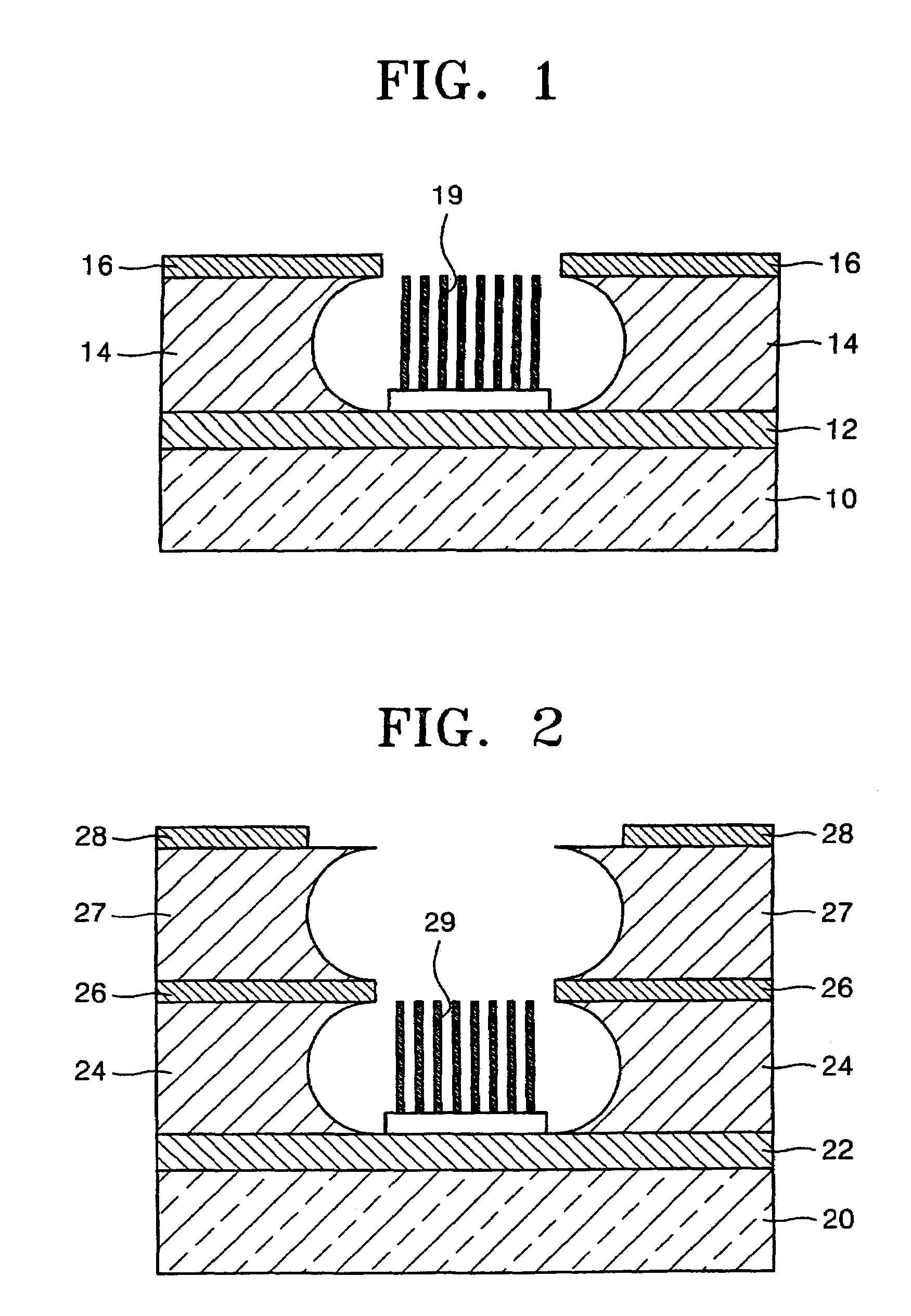
[0034]Turning now to the figures, FIG. 1 illustrates the structure of an FED. Referring to FIG. 1, the FED includes a substrate 10, a cathode electrode 12 formed on the substrate 10, an insulation layer 14 formed on the cathode electrode 12, and a gate electrode 16 formed on the insulation layer 14. A field emitter 19 is located in a hole perforating the insulation layer 14, through which part of the cathode electrode 12 is exposed.

[0035]In the FED of FIG. 1, however, desired pixels cannot radiate desired colors of light beams without controlling the trajectory of an electron beam emitted from the field emitter 19. Therefore, it is necessary to precisely control the trajectory of an electron beam emitted from the field emitter so that electrons emitted from the field emitter 19 can precisely arrive at pixels where they are supposed to arrive having an anode electrode coated with a fluorescent material.

[0036]There are two different techniques of controlling the trajectory of an elect...


PUM


Abstract

A novel field emission display (FED) and a novel method for making the same. The FED includes a substrate, a cathode electrode and a focus electrode formed on the same level with each other on the substrate, an insulation layer formed on the cathode electrode and the focus electrode such that the cathode electrode and the focus electrode are partially exposed through the insulation layer, a field emitter formed at the cathode electrode exposed by the insulation layer, and a gate electrode formed on the insulation layer. The field emitter being formed on the same layer and of the same material and at the same time as the cathode electrode.

Description

CLAIM OF PRIORITY[0001]This application makes reference to, incorporates the same herein, and claims all benefits accruing under 35 U.S.C. §119 from an application for FIELD EMISSION DISPLAY AND METHOD OF MANUFACTURING THE SAME earlier filed in the Korean Intellectual Property Office on 25 Nov. 2003 and there duly assigned Serial No. 2003-84180.BACKGROUND OF THE INVENTION[0002]1. Field of the Invention[0003]The present invention relates to a field emission display (FED) and a method of manufacturing the same, and more particularly, to an FED that can efficiently focus electron beams and a method of manufacturing the same.[0004]2. Description of the Related Art[0005]Display devices, which account for one of the most important parts of conventional data transmitting media, have been used in personal computers and television receivers. The display devices include cathode ray tubes (CRTs), which use high-speed heat electron emission, and flat panel displays, such as liquid crystal displ...

Claims


Application Information

Patent Timeline
Patent Type & Authority Patents(United States)
IPC IPC(8): H01J1/62H01J1/304H01J63/04H01J1/30H01J9/02H01J29/46H01J29/48H01J31/12
CPCH01J9/148H01J29/467H01J29/481H01J31/127C01B32/05H01J1/30
Inventor HAN, IN-TAEKOH, TAE-SIK
Owner SAMSUNG SDI CO LTD
Learn More