Surface conduction electron emitter display

a surface conduction electron and emitter technology, applied in the field of image forming apparatus, can solve the problems of image deterioration, light-emission position shift, image deterioration, etc., and achieve the effect of suppressing the position shift of the arrival position and high resistan

Inactive Publication Date: 2009-06-16
CANON KK
View PDF45 Cites 3 Cited by
  • Summary
  • Abstract
  • Description
  • Claims
  • Application Information

AI Technical Summary

Benefits of technology

[0015]In view of the foregoing, an object of the invention is to prevent irregular shift of the electron beam emitted from the electron-emitting device adjacent to the spacer when the plate-shaped spacer coated with an antistatic high resistance film is used. Another object of the invention is to suppress the position shift of the arrival position of the electron beam emitted from the adjacent electron-emitting device even if the spacer arranging position is slightly shifted. Another object of the invention is to adapt the spacer having the same configuration to various apparatus modes.

Problems solved by technology

However, the spacer is charged to affect an electron beam orbit near the spacer, which generates a problem in that light-emission position is shifted.
This causes the image deterioration such as a decrease in luminance and bleeding in pixels near the spacer.
For example, the unpredictable distortion is generated between the first-substrate wiring and the second-substrate electrode, a foreign matter exists on the first-substrate wiring and the second-substrate electrode, and an unintentional burr is generated in the wring or the electrode.
Therefore, the contact is not continuously achieved between the high resistance film of the spacer and the wiring or the electrode, and the position in which the high resistance film of the spacer is not partially in contact with the wiring or the electrode is generated, which causes the insufficient electrical contact.
Particularly, in the wiring produced by the inexpensive manufacturing method, sometimes there is the partial difference in the surface shape, and the electrical contact failure is easy to be generated.
In the above case, not only the charge of the spacer is not sufficiently eliminated, but also the irregular change is generated in the potential distribution of the spacer surface, which results in the problem that the electron beam orbit does not corresponds to the design.
Therefore, an arrival position of the electron beam radiated from the adjacent electron-emitting device is easily largely disturbed due to misalignment in arranging the spacer.
It is also found that the exposure of the spacer electrode to the side face of the space causes the discharge to largely decrease image quality.
In order to prevent the large decrease in image quality, it is necessary that the spacer electrode is not exposed to the side face of the spacer, or it is necessary that the spacer is arranged with high accuracy, which causes the cost increase.

Method used


Image

  • Surface conduction electron emitter display
  • Surface conduction electron emitter display
  • Surface conduction electron emitter display

Examples


example 1

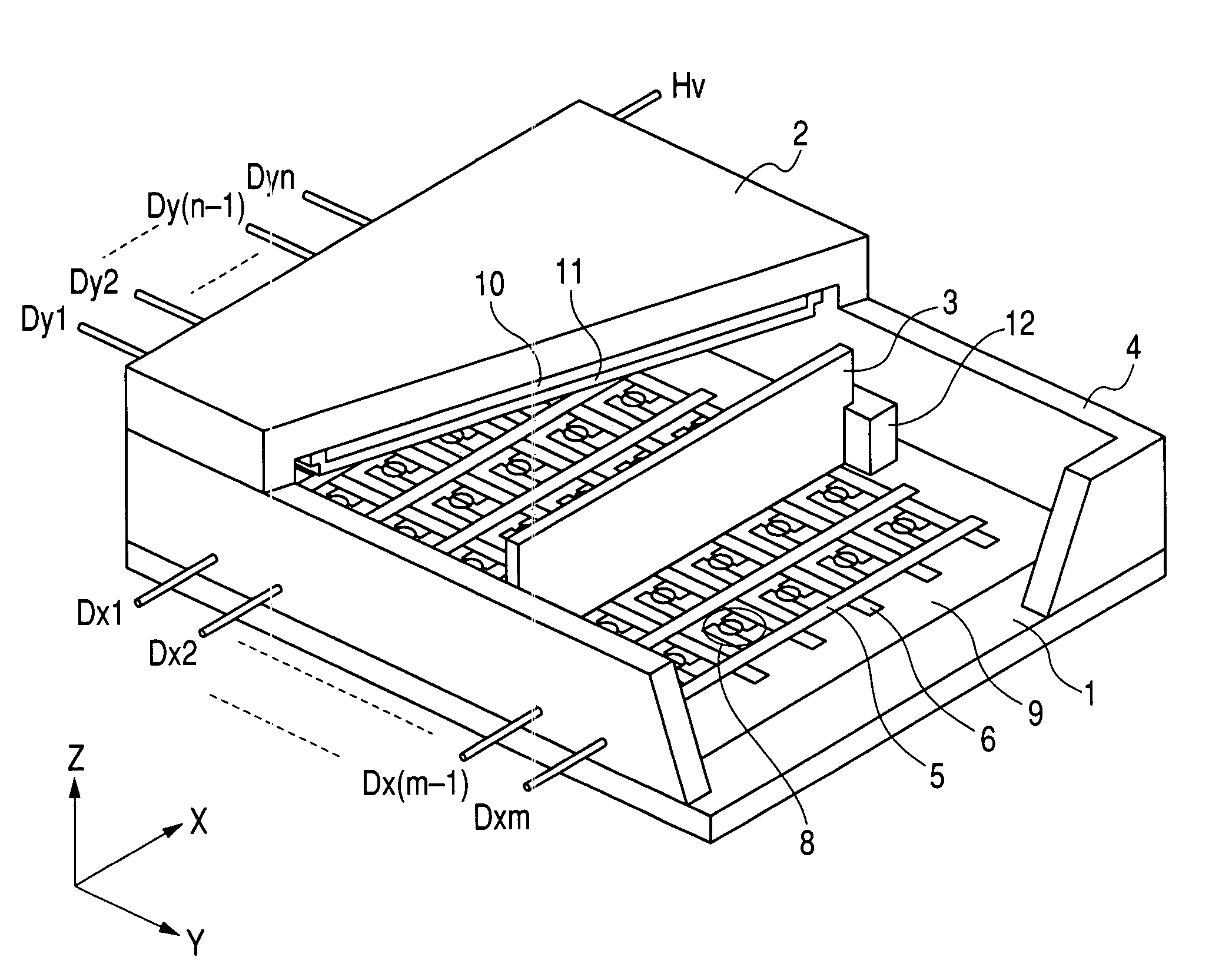
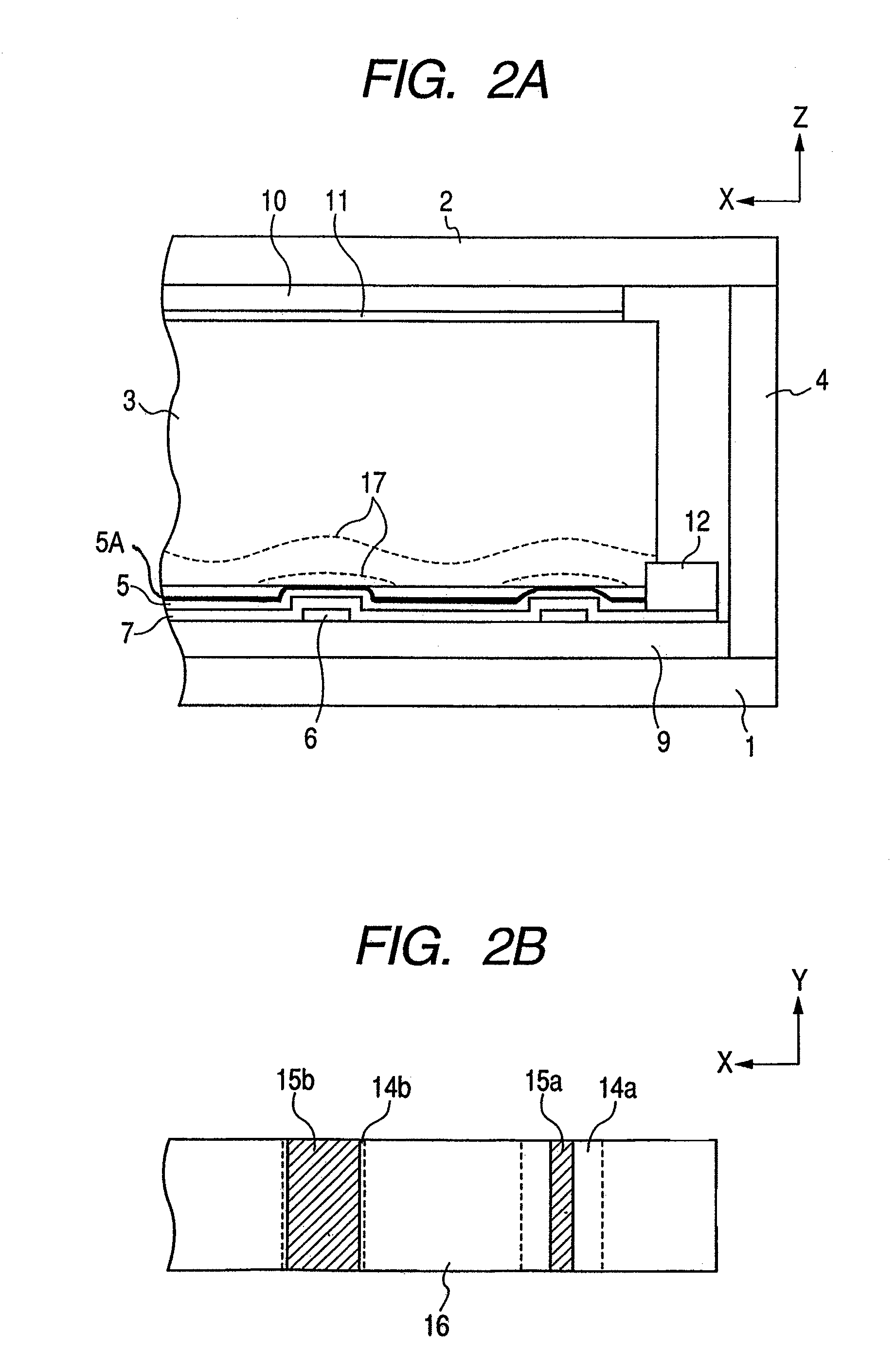
[0085]In the display panel described in the embodiment, PD 200 (produced by Asahi Glass Co., Ltd.) is used as the substrate 51 of the spacer 3, and tungsten nitride / germanium nitride compound (WGeN) is deposited as the high resistance film 52 by simultaneously sputtering a tungsten target and a germanium target in nitrogen gas. At this point, deposition is performed by rotating the substrate 51 of the spacer 3. Therefore, the film thickness is 200 nm across the entire surface, and the sheet resistance is 2.5×10¹² Ω / □. The thickness of the spacer 3 is set at 300 μm, and the height (Z-direction length) is set at 2.4 mm.

[0086]A SiO2 layer having the thickness of 0.5 μm is sputtered on the surface of the cleaned soda lime glass to form the rear plate 1. The device electrodes of the surface conduction electron-emitting device are formed on the rear plate 1 by the sputtering deposition method and the photolithography. For the material, Ti having the thickness of 5 nm and Ni having the thi...


PUM


Abstract

The invention provides an image forming apparatus in which orbit shift can be prevented to perform good image display in an electron beam emitted from the electron-emitting device adjacent to the spacer when an antistatic spacer coated with a high resistance film is used. A surface shape is controlled by forming a fine particle film on the surface of a row directional wiring 5 in which a spacer 3 is arranged, the electron emission is realized from electron-emitting areas 14a and 14b near contacting areas 15a and 15b in a non-contacting area 16 in which the spacer 3 is not in contact with the row directional wiring 5, and the non-contacting area 16 of the spacer 3 is irradiated with the electron to decrease a potential, which allows a good equipotential line 17 to be formed.

Description

BACKGROUND OF THE INVENTION[0001]1. Field of the Invention[0002]The present invention relates to an image forming apparatus which is used as, e.g. a display panel. More particularly, the invention relates to the image forming apparatus in which a spacer is sandwiched along wiring between a first substrate, which has plural electron-emitting devices and the wiring for driving the electron-emitting devices, and a second substrate, which has an electrode defined at a voltage higher than that of the wiring.[0003]2. Related Background Art[0004]Generally, in the image forming apparatus in which the first substrate on the electron source side and the second substrate on the display surface side are arranged in an opposite manner while separated from each other, the spacer made of an insulating and the second substrate in order to withstand atmospheric pressure. However, the spacer is charged to affect an electron beam orbit near the spacer, which generates a problem in that light-emission ...

Claims


Application Information

Patent Timeline
Patent Type & Authority Patents(United States)
IPC IPC(8): H01J1/62H01J1/00H01J1/05H01J1/14H01J9/18H01J9/24H01J29/02H01J29/86H01J31/12
CPCH01J1/316H01J9/185H01J9/242H01J29/028H01J29/864H01J31/127H01J2201/3165H01J2329/864H01J2329/8645H01J2329/8655H01J2329/8665H01J1/30H01J31/12
Inventor ANDO, YOICHI
Owner CANON KK
Why Eureka
Try Eureka