Wide-band antenna coupled spectrometer using CMOS transistor

a spectrometer and wide-band technology, applied in the field of cmos spectrometers, can solve the problems of often affected wavelength accuracy and difficult broad band sensitivity of spectrometers, and achieve the effect of inexpensive contact possibilities for antennas

Inactive Publication Date: 2009-06-16
GLOBALFOUNDRIES INC
View PDF15 Cites 8 Cited by
  • Summary
  • Abstract
  • Description
  • Claims
  • Application Information

AI Technical Summary

Benefits of technology

[0009]The present invention provides chip based spectrometers which are operable and sensitive across wide frequency ranges, thus useable for many different applications. The spectrometer makes use of multiple antennas, each configured to be responsive to a selected frequency or range of frequencies. All of these multiple antennas can be easily realized as part of a single chip, thus providing a very compact spectrometer. Further, due to the very small size of the necessary antennas, a large number of antennas may exist on the chip, thus providing a broad range of responsiveness. Each antenna can easily be positioned relative to a related CMOS transistor, resulting in the effective operation of the device as a broad band spectrometer.
[0011]As outlined above, the incorporation of multiple antenna based bolometers allows for detecting a broader spectrum of IR radiation thus providing spectrometer capabilities. That said, each of these antennas are typically specifically designed and configured to detect IR radiation within a specific frequency range. This is primarily due to the geometry of the antenna itself which is sensitive to a particular frequency. By selecting a narrow band high Q antenna, it is possible to construct bolometers which are sensitive to a very focused frequency range. A large number of antennas with each having a slightly different mechanical dimension allows for the coverage of a large frequency range.
[0012]As mentioned above, the broad band sensitivity necessary for spectrometers can often be challenging. The present invention addresses this challenge by providing wavelength accuracy due to the mechanical dimensions of each particular antenna. As the physical structure making up the antenna can be easily controlled on a silicon chip, accurate antennas are thus produced. Further, wavelength accuracy is often affected by dielectric properties of materials used in the back end of the line CMOS process (BEOL). However, in a spectrometer using a known substance and having known absorption lines, calibration can easily be performed. In addition, drift will thus affect all antennas similarly, and thus not have effects on the overall spectrometer operation.
[0014]Each detector according to this aspect of the invention receives the electromagnetic waves by means of the antenna and converts the received electromagnetic radiation into heat by means of the termination section of the semiconductor element. The termination section functions as termination resistor of the antenna. The heat produced in the termination section is used for heating a temperature-sensitive part of the semiconductor device. The temperature-sensitive part can be any part of the semiconductor-element that comprises a measurable temperature-dependent characteristic. Advantageously, the termination section is arranged in the proximity of the temperature-sensitive part. Advantageously, the termination section heats the temperature-sensitive part selectively. In other words, the termination section does not heat the complete semiconductor element evenly or uniformly, but produces the heat at or in the proximity of the temperature sensitive part. In other words, the produced heat is focused on the area of the temperature sensitive part. Such a focusing of the heat on the temperature-sensitive part enhances the sensitivity of the detector.
[0016]According to this embodiment one of the electrodes of the transistor acts as termination resistor for the antenna. The respective electrode is coupled at two termination points to an arm of the antenna. The respective electrode comprises preferably a gap between the two termination points. In other words, the respective electrode comprises two parts, wherein each part is connected to one of the arms of the antenna. The termination section or termination resistor respectively can be established by using the semiconductor path between the two termination points or the two electrode parts respectively. The termination points are advantageously arranged at opposite sides of the transistor. This provides space for establishing the required matching impedance between the termination points via the semiconductor substrate. The transistor electrodes offer inexpensive contact possibilities for the antenna.

Problems solved by technology

As mentioned above, the broad band sensitivity necessary for spectrometers can often be challenging.
Further, wavelength accuracy is often affected by dielectric properties of materials used in the back end of the line CMOS process (BEOL).

Method used


Image

  • Wide-band antenna coupled spectrometer using CMOS transistor
  • Wide-band antenna coupled spectrometer using CMOS transistor
  • Wide-band antenna coupled spectrometer using CMOS transistor

Examples


Embodiment Construction

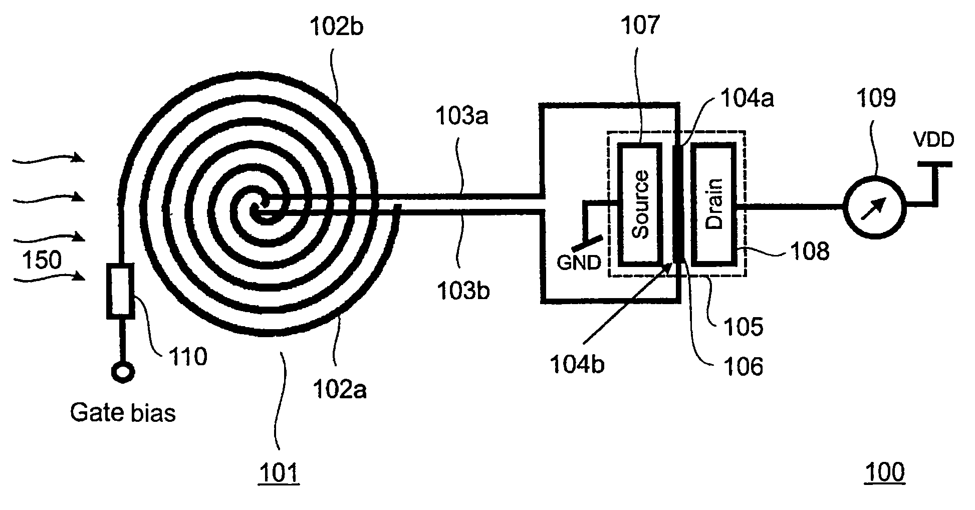
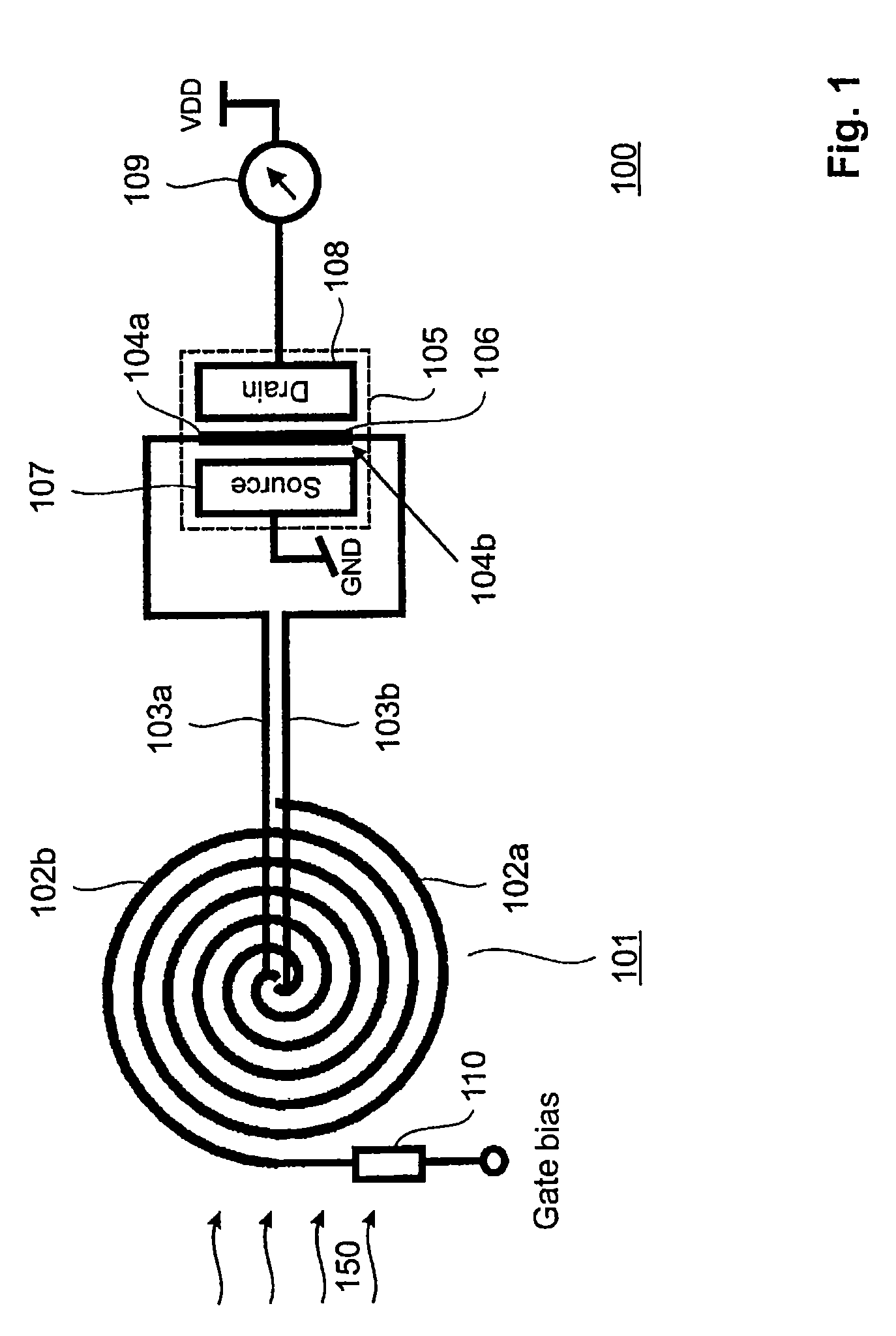
[0029]FIG. 1 shows a schematic illustration of a detector 100 for detecting electromagnetic waves 150 according to an embodiment of the present invention. The detector 100 is in particular suitable for detecting electromagnetic waves 150 with a frequency in the THz range. The detector 100 comprises an antenna 101 for receiving the electromagnetic waves 150. The antenna 101 can be e.g. a planar broadband antenna with a ground plane. The antenna 101 is in particular suited to receive electromagnetic waves in a wavelength range between 3 μm and 15 μm. The antenna 101 comprises a first arm 102a and a second arm 102b. The first arm 102a is connected by means of a first via 103a to a first termination point 104a and the second arm 102b is connected by means of a second via 103b to a second termination point 104b. The first termination point 104a and the second termination point 104b are contact points for contacting a gate 106 of a Field Effect Transistor (FET) 105. Thus the gate 106 of t...


PUM

PropertyMeasurementUnit
wavelength rangeaaaaaaaaaa

Abstract

To create a broad band spectrometer, a plurality of individual antenna based bolometers are fabricated on the surface of a single spectrometer chip, each bolometer having an individual antenna which is sized differently from all others, thus being responsive to a generally unique frequency of radiation. Each antenna is coupled to a related transistor, which is easily formed using CMOS technology. The antennas are connected to opposite sides of a transistor gate, thus creating a termination resistor for the particular antenna. Multiple outputs from the various antennas are then coupled, thus providing responsiveness to electromagnetic radiation of a very broad spectrum.

Description

RELATED APPLICATIONS[0001]This application is a continuation-in-part of U.S. patent application Ser. No. 11 / 774,087 entitled DETECTOR FOR DETECTING ELECTROMAGNETIC WAVES, filed Jul. 6, 2007.FIELD OF THE INVENTION[0002]The present invention relates to a chip based spectrometer utilizing CMOS technology. More specifically, the present invention relates to a CMOS spectrometer made up of multiple antenna elements, with each antenna element operatively coupled to the gate of a corresponding CMOS transistor.BACKGROUND OF THE INVENTION[0003]Detectors and sensors of all different types are utilized in virtually every walk of life. The miniaturization and efficiency of any sensor is a continuous goal for device designers. Stated alternatively, it is almost always beneficial to design and develop sensors and detectors which are more efficient and which can be packaged as smaller devices. By developing small efficiently operating sensors, various additional applications are typically made poss...

Claims


Application Information

Patent Timeline
Patent Type & Authority Patents(United States)
IPC IPC(8): G01R31/00
CPCG01J3/2803H01Q9/27H01Q11/105H01L31/08G01J2001/4295H01L27/1446Y10T29/49002
Inventor MORF, THOMAS E.TOIFL, THOMAS H.
Owner GLOBALFOUNDRIES INC
Why Eureka
Try Eureka