Method and apparatus for growing high quality silicon single crystal, silicon single crystal ingot grown thereby and wafer produced from the same single crystal ingot

a technology of high-quality silicon single crystal and single crystal ingot, which is applied in the direction of crystal growth process polycrystalline material growth, etc., can solve the problem of reducing the yield of the device, unable to efficiently control the temperature gradient or oxygen concentration of the and unable to produce high-quality si single crystal ingot and wafer. problem, to achieve the effect of high productivity

Active Publication Date: 2009-07-14
LG SILTRON
View PDF25 Cites 8 Cited by
  • Summary
  • Abstract
  • Description
  • Claims
  • Application Information

AI Technical Summary

Benefits of technology

[0017]Accordingly, the present invention has been made to solve the above-mentioned problems occurring in the prior art, and an object of the present invention is to provide a method capable of producing a Si single crystal ingot with a high productivity while controlling the Si single crystal ingot to have various oxygen concentrations.
[0020]Another object of the invention is to provide a method for growing a high quality Si single crystal ingot having a high productivity.
[0021]Yet another object of the invention is to provide an apparatus for growing a high quality Si single crystal ingot having a high yield.
[0025]Preferably, the temperature of silicon melt rises gradually in proportion to the distance from a single crystal ingot up to a hottest point and descends gradually from the hottest point when measured along an axis parallel with a longitudinal direction of the single crystal ingot starting from an interface between silicon melt and the single crystal ingot, and the unbalanced magnetic field is adapted to minimize oxygen dissolution from the crucible and promote melt convection from a portion of silicon melt which is most adjacent to the heater toward a center of the interface or a hot region surrounding the hottest point.
[0032]Preferably, the magnet is adapted to induce the magnetic field to minimize the dissolution of oxygen from the crucible.

Problems solved by technology

However, adjustment of several process parameters of the prior art cannot efficiently control the temperature gradient or oxygen concentration of a Si single crystal ingot.
So, it has been impossible to produce a high quality Si single crystal ingot and wafer with low point defect concentration that have oxygen concentrations desirable to customers.
For example, Crystal Originated Pit (COP), as a type of point defects with agglomerated vacancies worsens Gate Oxide Integrity (GOI), thereby dropping device's yield.
Furthermore, GOI may worsen if micro precipitates depending on oxygen and vacancy concentration have occurred in the active device region.
The MBD occurring during heat treatment of a semiconductor device is harmful for the active device area, but improves device's yield by gettering of metal impurities existing in the wafer surface and the active device region.
If out-diffusion does not take place by a sufficient degree around the outer circumference of the single crystal ingot, an interstitial crystal defect such as LDP occurs.
On the other hand, dropping the cooling rate of crystal for the purpose of interstitial out-diffusion further requires installation of additional hot zones.
This decreases the growth rate of the single crystal ingot, thereby lowering productivity.
However, these techniques have drawbacks in that either they require additional investment or the high quality single crystal is not actually produced.
However, such conventional techniques have not disclosed using an unbalanced magnetic field in order to control oxygen concentration in a high quality Si single crystal ingot that is free of agglomerated crystal defects.
Moreover, according to the afore-mentioned techniques, the sought-after high quality single crystal ingot can be produced only with a low yield.

Method used


Image

  • Method and apparatus for growing high quality silicon single crystal, silicon single crystal ingot grown thereby and wafer produced from the same single crystal ingot
  • Method and apparatus for growing high quality silicon single crystal, silicon single crystal ingot grown thereby and wafer produced from the same single crystal ingot
  • Method and apparatus for growing high quality silicon single crystal, silicon single crystal ingot grown thereby and wafer produced from the same single crystal ingot

Examples


example 1

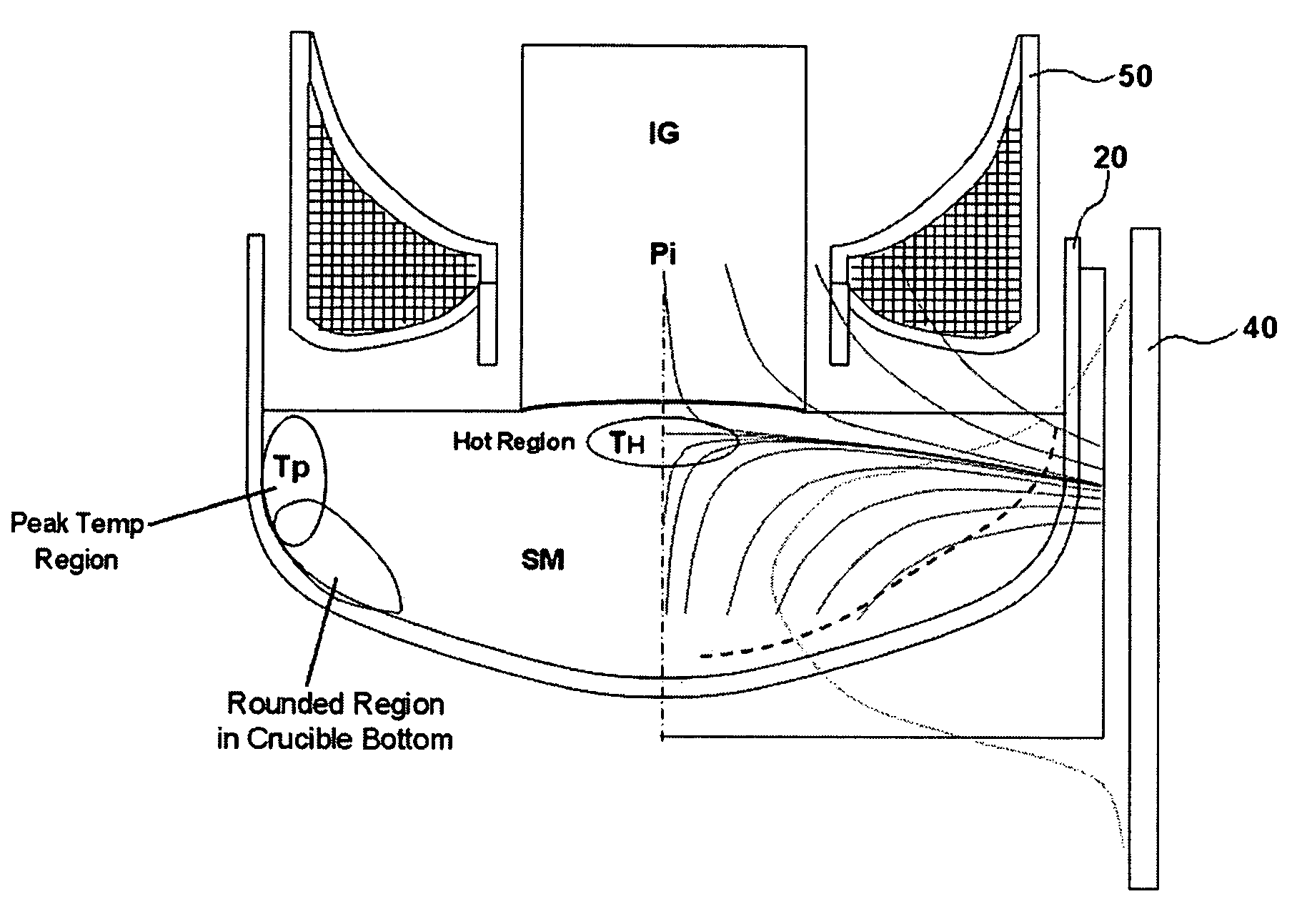
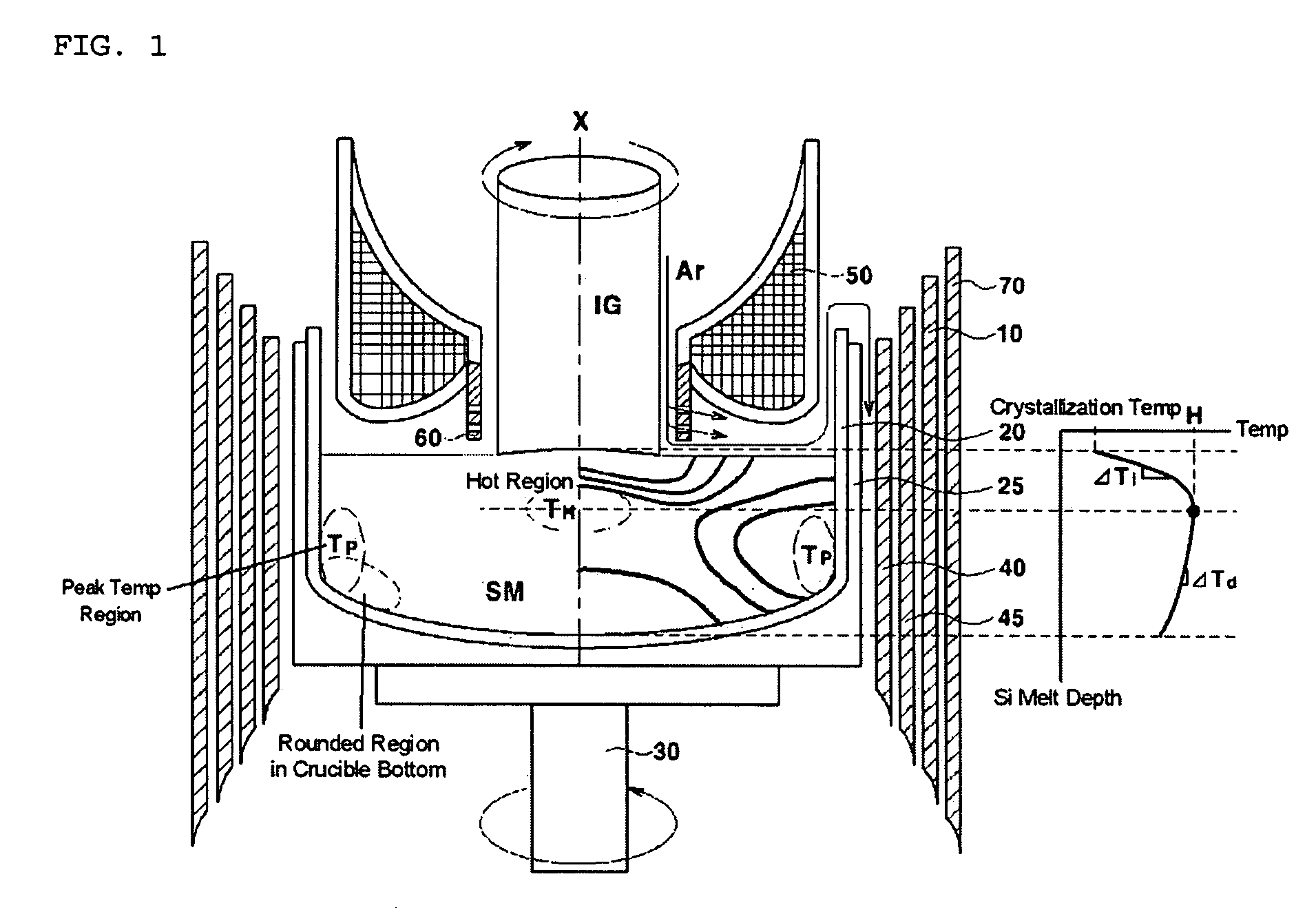
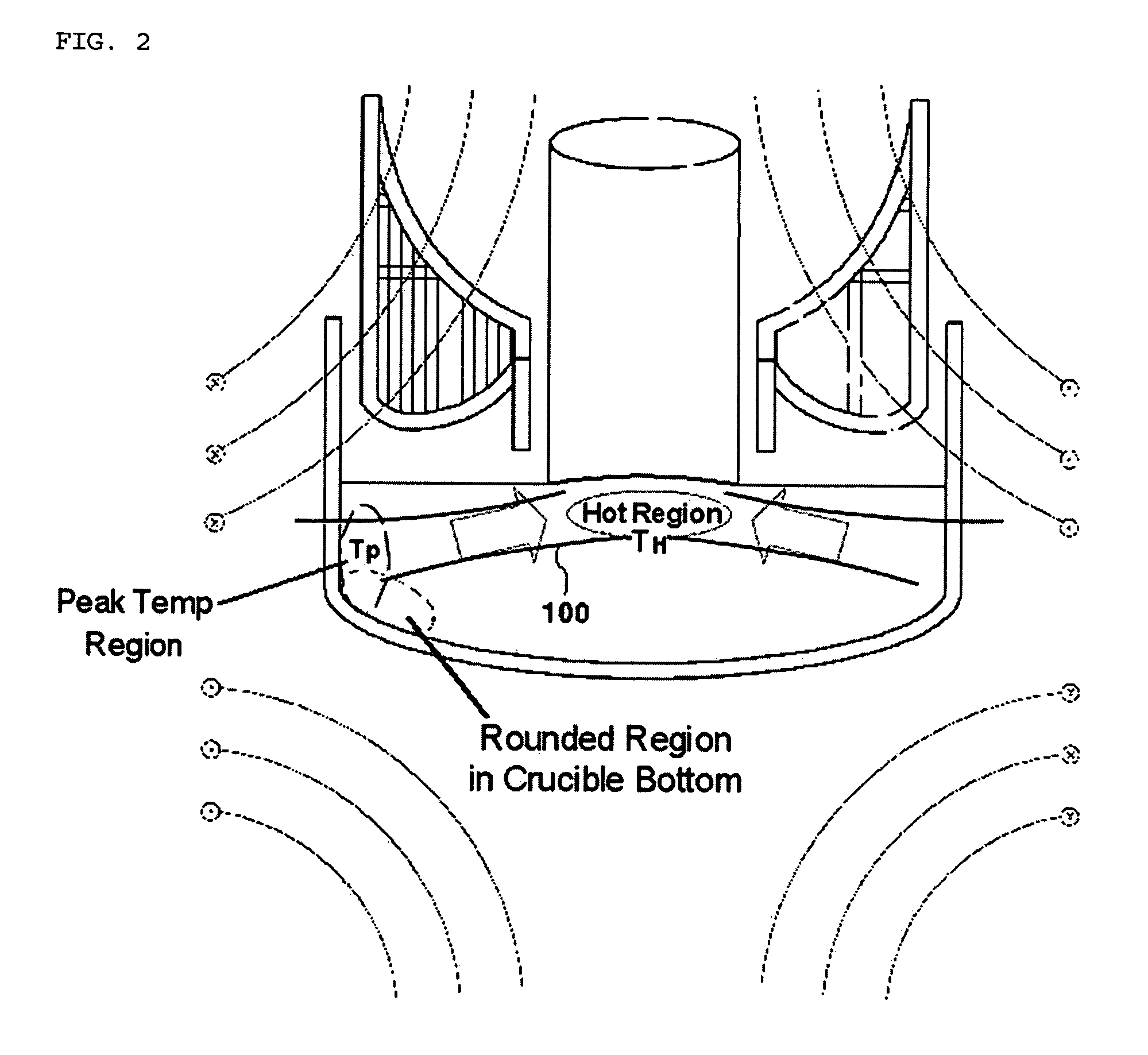
[0113]Si single crystal ingot having asymmetric point defect concentration distribution where interstitial is dominant in ingot center and vacancy is dominant in outer periphery.

[0114]The temperature distribution of Si melt was controlled by adjusting the rotation speed of a single crystal ingot and the rotation speed of a crucible. The rotation speed of the single crystal ingot was 13 rpm to 17 rpm, and the rotation speed of the crucible was 0.3 rpm to 0.8 rpm. In order to effectively control point defect concentration in the Si single crystal ingot, the temperature distribution of Si melt was controlled instead of the Si single crystal ingot.

[0115]By increasing the vertical temperature gradient of Si melt from the growth interface of the Si single crystal ingot to a 10 mm to 100 mm depth portion, limit pulling speed for interstitial-to-vacancy transition in the ingot center was enhanced by a large value.

[0116]A vertical section sample of the grown up single crystal ingot was picke...

example 2

[0118]Si single crystal ingot having asymmetric point defect concentration distribution where point defect is extremely controlled

[0119]The temperature distribution of Si melt was improved by adjusting the center position and magnetic field strength of a CUSP magnetic field in addition to the rotation speed of a single crystal ingot and the rotation speed a crucible. The single crystal ingot and the crucible were given with the same rotation speeds as in Example 1. The magnetic field strength was 100 gauss at the solid-liquid interface center and 190 gauss at the rounded bottom portion.

[0120]The temperature distribution of Si melt is adjusted instead of that of the Si single crystal ingot in order to extremely control the point defect concentration. That is, by increasing the vertical temperature gradient of Si melt from the growth interface of the Si single crystal ingot to 30 mm depth point of Si melt, the pulling speed of the single crystal ingot was remarkably enhanced so that b...

example 3

[0123]High quality Si single crystal ingot having asymmetric point defect concentration distribution where oxygen concentration is controlled

[0124]By setting unbalanced CUSP upper and lower magnetic field strengths, in addition to the rotation speed of a single crystal ingot and the rotation speed of a crucible, heat transfer was made more efficient and oxygen concentration was lowered. The single crystal ingot and the crucible were given with the same rotation speeds as in Example 1. The magnetic field strength was 20 gauss at the solid-liquid interface center and 340 gauss at the rounded bottom portion.

[0125]That is, the lower magnetic field strength was enhanced to lower oxygen concentration and the upper magnetic field strength was adjusted relatively weak so that heat could be transferred from a heater to the solid-liquid interface via the shortest path. In this case, the magnetic fields were adjusted to maintain the shape of heat channels uniform.

[0126]A vertical section sampl...


PUM

PropertyMeasurementUnit
magnetic fieldaaaaaaaaaa

Abstract

The invention relates to a technique for producing a high quality Si single crystal ingot with a high productivity by the Czochralski method. The technique of the invention can control the magnetic field strength of an oxygen dissolution region different from that of a solid-liquid interface region in order to control the oxygen concentration at a desired value.

Description

BACKGROUND OF THE INVENTION[0001]1. Field of the Invention[0002]The present invention relates to a high quality silicon (Si) single crystal ingot having desirable oxygen concentration, and more particularly, a high quality Si single crystal ingot and wafer and a growth method and apparatus thereof, in which the temperature distribution and the oxygen concentration distribution of Si melt are controlled independently from each other during the growth of an Si single crystal ingot by the Czochralski method in order to produce a high quality Si single crystal ingot and wafers which have controlled growth defects and oxygen concentrations desirable to customers.[0003]2. Description of the Prior Art[0004]As well known in the art, in order to grow a high quality silicon (Si) single crystal ingot that can enhance the yield of semiconductor devices, temperature control has mainly been conducted on high temperature distribution of the single crystal ingot after crystallization. This is done ...

Claims


Application Information

Patent Timeline
Patent Type & Authority Patents(United States)
IPC IPC(8): C30B15/20
CPCC30B15/30C30B29/06C30B30/04Y10T117/1068Y10T117/1072Y10T117/1052Y10T117/1088C30B15/00
Inventor CHO, HYON-JONG
Owner LG SILTRON
Why Eureka
Try Eureka