Electromagnetic-wave shielding and light transmitting plate and manufacturing method thereof

Inactive Publication Date: 2009-07-14
BRIDGESTONE CORP
View PDF11 Cites 13 Cited by
  • Summary
  • Abstract
  • Description
  • Claims
  • Application Information

AI Technical Summary

Benefits of technology

[0013]The present invention provides an electromagnetic-wave shielding and light transmitting plate in which surfaces of portions of the transparent film at the apertures of the conductive pattern are covered by transparent resin. This electromagnetic-wave shielding and light transmitting plate has excellent surface flatness as compared to an electromagnetic-wave shielding and light

Problems solved by technology

In case of the transparent conductive film, however, it is difficult to achieve electric conduction relative to a panel body.
If the transparent co

Method used


Image

  • Electromagnetic-wave shielding and light transmitting plate and manufacturing method thereof
  • Electromagnetic-wave shielding and light transmitting plate and manufacturing method thereof

Examples


example 1

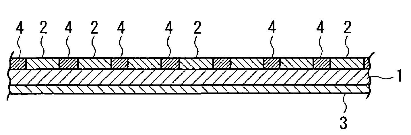
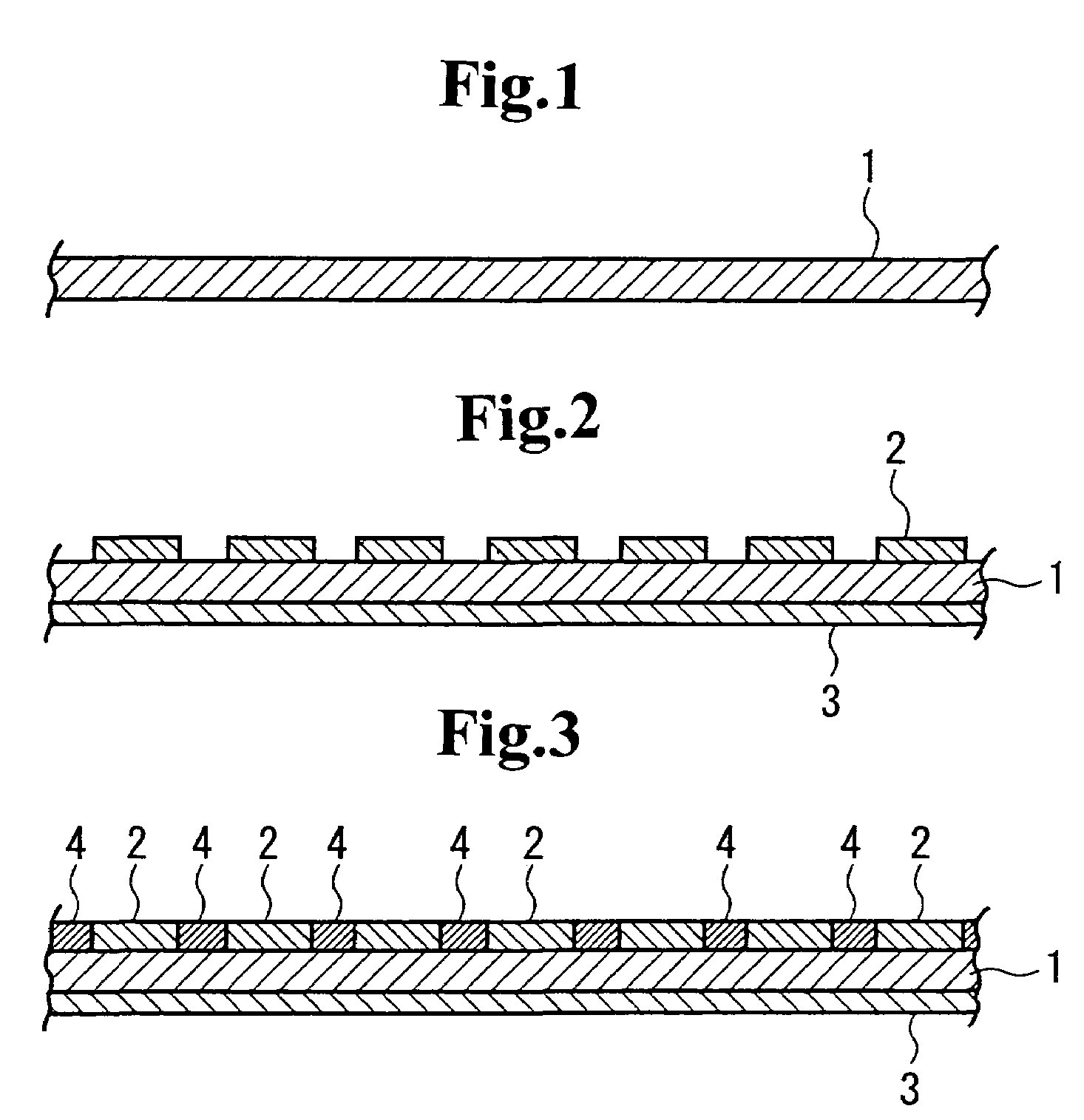
[0035]Dots were printed on a triacetylcellulose film of 100 μm in thickness by using 20% solution of plating resist (SM1798JR-1 available from Fujikura Kasei Co., Ltd.) mainly containing acrylic polymer. Each dot was a square shape of which one side was 234 μm and the space between adjacent dots was 20 μm. The dots were arranged in a square grid. The printing thickness after dried was about 2 μm. A backside coating layer was formed with the same plating resist on the entire back surface of the film in such a manner as to have a thickness after dried of 2 μm.

[0036]Copper was plated on the film exposed area not covered by the dots by means of the electroless plating in such a manner as to have an average thickness of 2 μm. Finally, blackening treatment was applied by means of oxidation treatment, thereby obtaining an electromagnetic-wave shielding and light transmitting plate. It should be noted that the copper is not attached to the plating resist at all.

[0037]The conductive layer on...


PUM

PropertyMeasurementUnit
Fractionaaaaaaaaaa
Fractionaaaaaaaaaa
Thicknessaaaaaaaaaa

Abstract

To manufacture an electromagnetic-wave shielding and light transmitting plate having a conductive pattern of which line width is narrow and open area ratio is high, a negative pattern 2 composed of dots is printed on a transparent film 1 having a high affinity for a plated layer of a conductive material by using a transparent resin having a low affinity for the plated layer and a backside coating layer 3 is formed by printing a transparent resin on the entire back surface of the transparent film 1. Then, a conductive material layer is formed by electroless plating to cover the film exposed surface not covered by the negative pattern 2 of the film 1, thereby forming the conductive pattern 4. After that, the blackening treatment is conducted, thereby obtaining the electromagnetic-wave shielding and light transmitting plate.

Description

CROSS REFERENCE TO RELATED APPLICATION[0001]This is a continuation application of PCT / JP02 / 11544 filed on Nov. 6, 2002.FIELD OF THE INVENTION[0002]The present invention relates to an electromagnetic-wave shielding and light transmitting plate which can be suitably used as a front filter for a PDP (plasma display panel) or a window sheet (for example, a bonding film) for a building such as a hospital where needs electromagnetic-wave shielding and to a manufacturing method of the same. More particularly, the present invention relates to an electromagnetic-wave shielding and light transmitting plate which comprises a film and a conductive pattern formed on the film and to a manufacturing method of the same.BACKGROUND OF THE INVENTION[0003]Plates having electromagnetic-wave shielding property and light transmission properties have been developed as front filters of equipment such as office automation equipment and communication equipment in order to shield electromagnetic wave produced ...

Claims


Application Information

Patent Timeline
IPC IPC(8): B05D5/12H05K9/00
CPCH05K9/0096
Inventor KOTSUBO, HIDEFUMIMORIMURA, YASUHIROTANUMA, ITSUO
Owner BRIDGESTONE CORP
Why Eureka
Try Eureka