Thin film solar cell configuration and fabrication method

a solar cell and thin film technology, applied in the field of thin film photovoltaic (pv) technology, can solve the problems of affecting device stability, affecting device stability, complex and hazardous vapor phase methods used in cigs deposition, etc., to reduce the number of cell components and processing steps, easy to scale up for mass production, and eliminate complexity and expense

Inactive Publication Date: 2009-07-14
MENEZES SHALINI
View PDF11 Cites 21 Cited by
  • Summary
  • Abstract
  • Description
  • Claims
  • Application Information

AI Technical Summary

Benefits of technology

[0026]The n-CIS PV device can eliminate the complexity and expense associated with the deposition and synthesis of the quaternary CIGS or higher order (CIGS+sulfur) compound and its expensive Mo contact layer. It eliminates the toxic CdS deposition and KCN etch. Reducing the number of cell components and processing steps can produce an ultra-simple, low-cost n-CIS PV cell that can be readily scaled for mass production.

Problems solved by technology

However, the current methods available for CIGS deposition use mainly vapor phase methods, which are complex, hazardous and extremely expensive.
The CuInS2 material has not demonstrated good PV performance even when produced by the more expensive vapor deposition techniques or in single crystal form.
The presence of many secondary phases also impacts the device stability.
Adapting the electrodeposition approach to the more efficient p-CIGS absorber to produce a cost effective flexible cell configuration poses many technical and economical challenges: (a) the p-CIGS device requires a sputtered Mo layer or Mo-foil contact, which is too expensive for large-scale terrestrial applications; (b) CIGS electrodeposition on Mo coated metal substrates requires a conducting diffusion barrier between Mo and the metal; (c) the co-electrodeposition of Ga, S and Na with Cu, In and Se is extremely difficult: many of these elements have to be added by vapor deposition.
These additional materials and process steps complicate the fabrication process and add higher costs.
The need for chemical bath deposition of a CdS buffer layer and KCN etch for the CIGS and CuInS2 based PV cells further add to the hazards and the waste disposal expense.
Light-blocking metallization was used to make the front contact to the device, which impeded its energy conversion efficiency assessment.

Method used


Image

  • Thin film solar cell configuration and fabrication method
  • Thin film solar cell configuration and fabrication method
  • Thin film solar cell configuration and fabrication method

Examples


Embodiment Construction

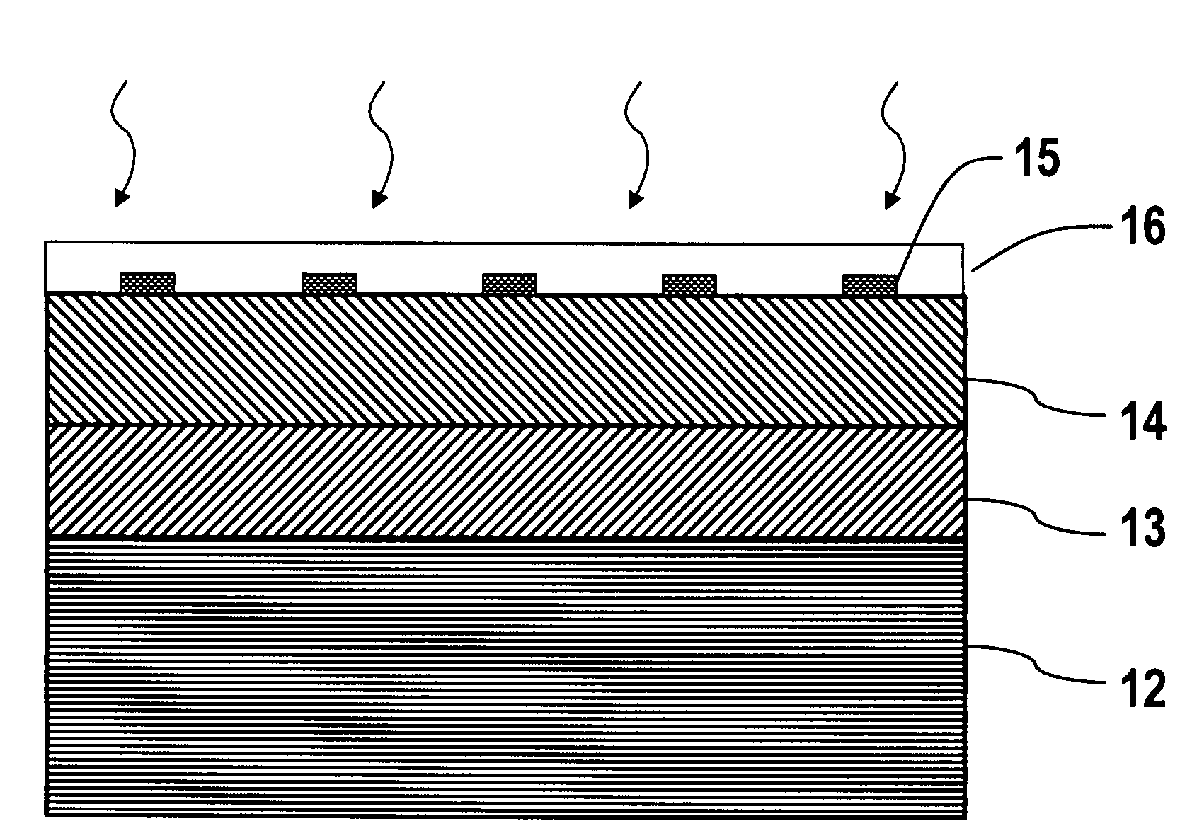
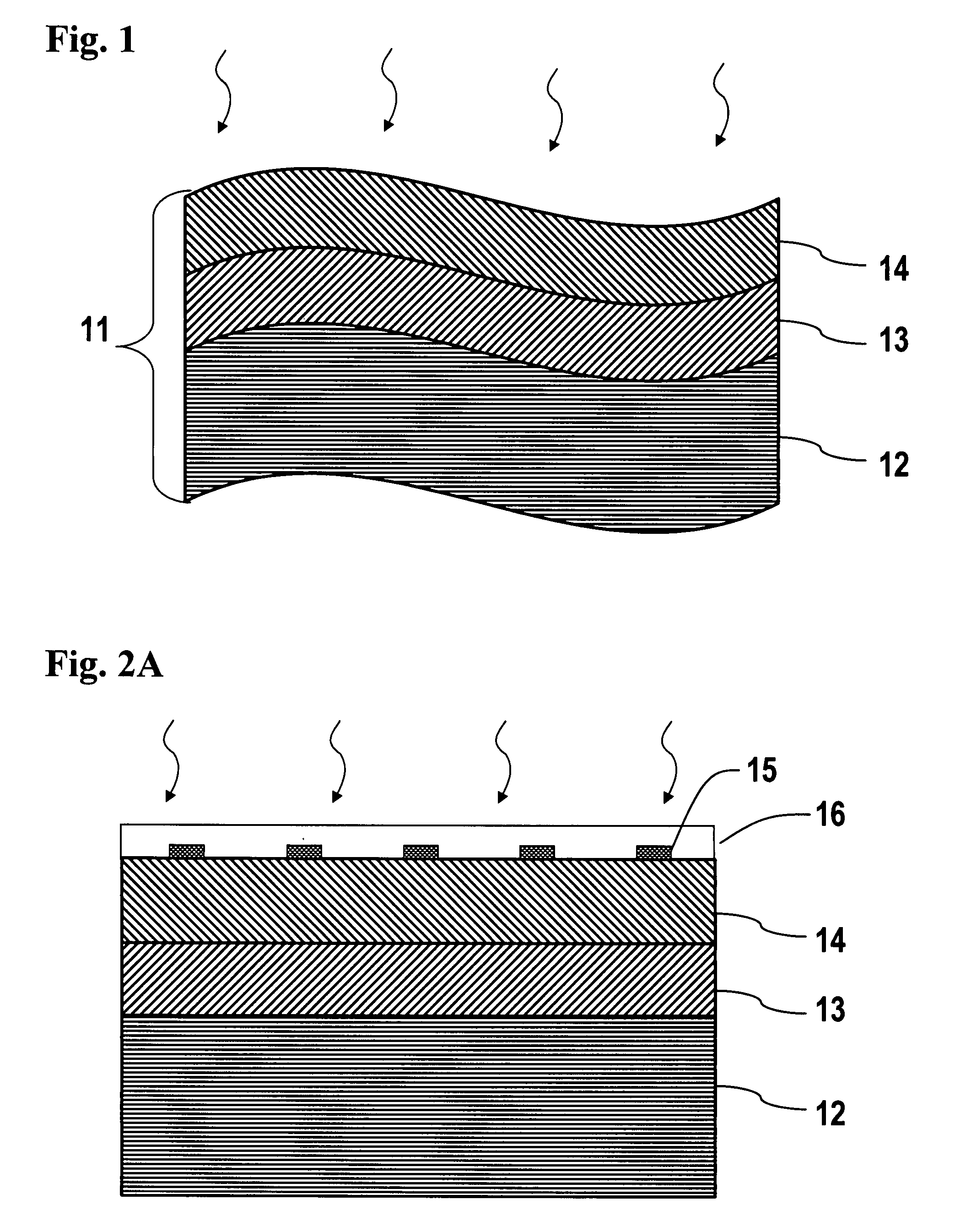
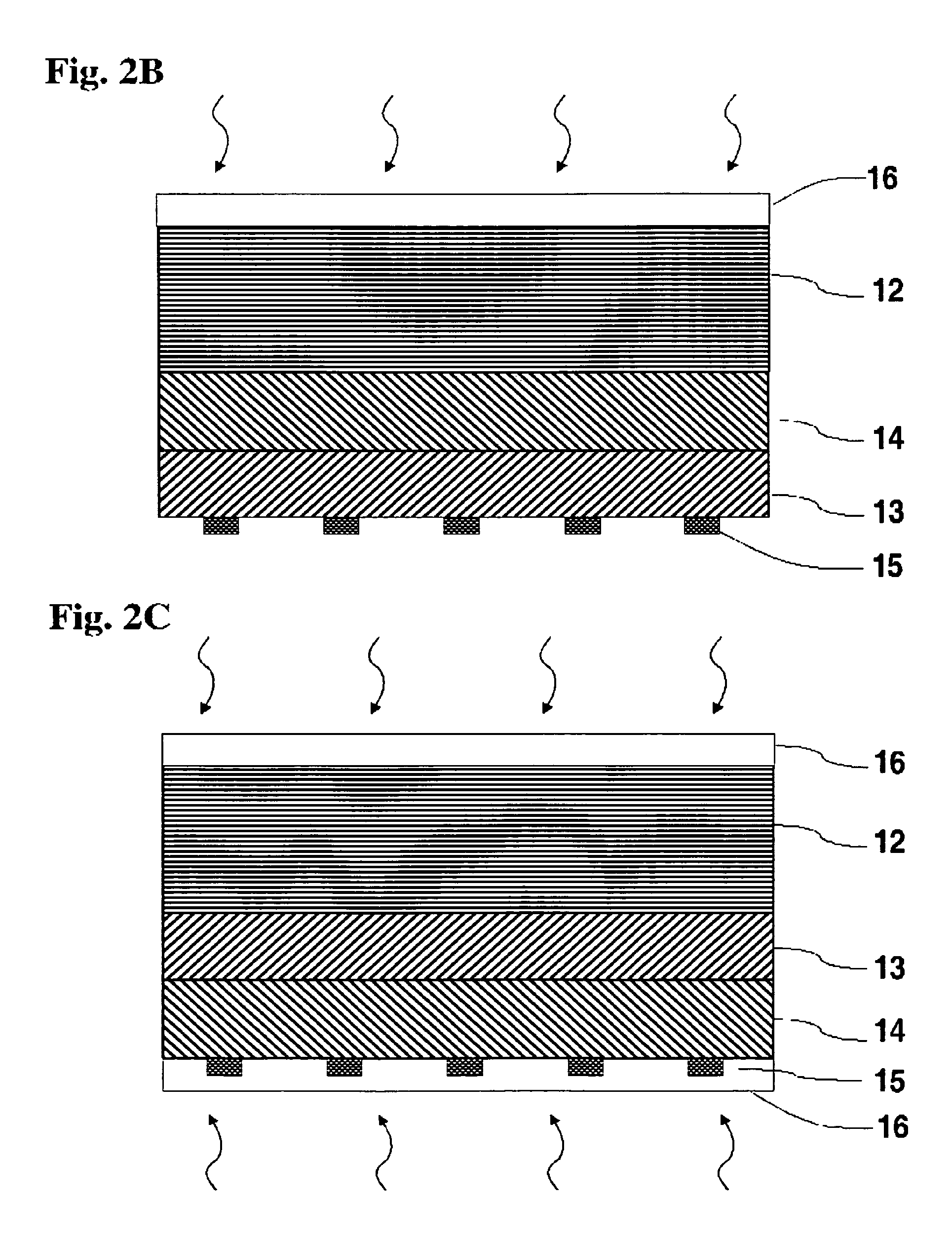
[0038]This invention adapts the n-CIS / p-CuISe3 heterojunction formation concept, described in U.S. Pat. No. 5,286,306 to a practical device that can be mass-produced for a wide range of applications. U.S. Pat. No. 5,286,306 is hereby incorporated by reference for its teachings to make an n-CuInSe2 based thin-film cell. This invention describes a new low-cost method to produce an n-CIS absorber layer on flexible substrates and subsequent process steps to fabricate the relevant cell components. It combines the electrochemical n-CIS / p-CuISe3 heterojunction formation concept with new materials and processes, such as: (I) flexible substrate, (II) roll-to-roll fabrication (III) electrodeposition for n-CIS, (IV) ODC absorber layer, (V) electrodeposited Cu-halide or pseudo-halide window and (VI) TCO front contact.

[0039]FIG. 1 shows a basic configuration of a flexible n-CIS solar cell 11 made in accordance with the present invention. It comprises a substrate 12 on which the n-type CIS absorb...


PUM


Abstract

A new photovoltaic device configuration based on an n-copper indium selenide absorber and a p-type window is disclosed. A fabrication method to produce this device on flexible or rigid substrates is described that reduces the number of cell components, avoids hazardous materials, simplifies the process steps and hence the costs for high volume solar cell manufacturing.

Description

CROSS-REFERENCE TO RELATED APPLICATIONS[0001]A provisional Patent Application No. 60 / 431,268, entitled “Flexible Solar Cell Configuration and Fabrication Method” was filed on Dec. 6, 2002 with the US Patent and Trademark Office.[0002]An Invention Disclosure entitled “New Approach and Configuration for a Low Cost Flexible CIS Thin film Solar Cell” conceived by Dr. Shalini Menezes was documented and witnessed on Jun. 29, 2000.STATEMENT REGARDING FEDERALLY SPONSORED RESEARCH OR DEVELOPMENT[0003]This invention was partly reduced to practice with Government support under a SBIR grant awarded by NSF and an EISG grant awarded by the California Energy Commission. The Government has certain rights in the invention.REFERENCE TO SEQUENCE LISTING, A TABLE, OR A COMPUTER PROGRAM LISTING COMPACT DISK APPENDIX[0004]Not applicable.BACKGROUND OF THE INVENTION[0005]The invention relates to the field of thin film photovoltaic (PV) technology. PV devices use sunlight to generate clean, reliable electri...

Claims


Application Information

Patent Timeline
Patent Type & Authority Patents(United States)
IPC IPC(8): H01L31/00
CPCH01L31/0322H01L31/18H01L31/0749Y02E10/541H01L21/02568H01L21/02614H01L21/02628Y02P70/50
Inventor MENEZES, SHALINI
Owner MENEZES SHALINI
Why Eureka
Try Eureka