Semiconductor strain sensor

a technology of micro-conductor and sensor, which is applied in the direction of fluid pressure measurement, fluid pressure measurement by electric/magnetic elements, instruments, etc., can solve the problems of thermal hysteresis, thermal stress, temperature drift, etc., in the output signals of the sensor, and achieve the effect of suppressing thermal hysteresis of the output voltag

Active Publication Date: 2009-07-21
MITSUBISHI ELECTRIC CORP
View PDF16 Cites 8 Cited by
  • Summary
  • Abstract
  • Description
  • Claims
  • Application Information

AI Technical Summary

Benefits of technology

[0007]The present invention aims to solve the above problems and an object of the present invention is to provide a semiconductor strain sensor that has superior temperature stability by separating a region of formation of an electrode from a diaphragm portion on which a piezoresistive element is formed to make the piezoresistive element less likely to be affected by thermal stresses from the electrode.
[0009]According to the present invention, because the electrode is disposed at a position on the outer frame portion that is separated by greater than or equal to 100 μm from the boundary between the diaphragm portion and the outer frame portion, the piezoresistive element is less likely to be affected by thermal stresses from the electrode, suppressing thermal hysteresis of the output voltage to less than or equal to 0.2 percent FS per sensor chip unit. Thus, 1 percent FS or less, which is demanded of control systems, can be met even after the semiconductor strain sensor has been assembled for on-board installation.

Problems solved by technology

The thermal expansion coefficient of aluminum is approximately 23.5 ppm / ° C., and the thermal expansion coefficient of single-crystalline silicon is approximately 2.5 ppm / ° C. Thus, because the thermal expansion coefficients of the electrodes and the semiconductor substrate differ greatly, one problem has been that the electrodes and the semiconductor substrate may warp if the ambient temperature at which the sensor is used changes, generating thermal stresses and giving rise to temperature drift, or thermal hysteresis, etc., in the output signals from the sensor.

Method used


Image

  • Semiconductor strain sensor
  • Semiconductor strain sensor
  • Semiconductor strain sensor

Examples


embodiment 1

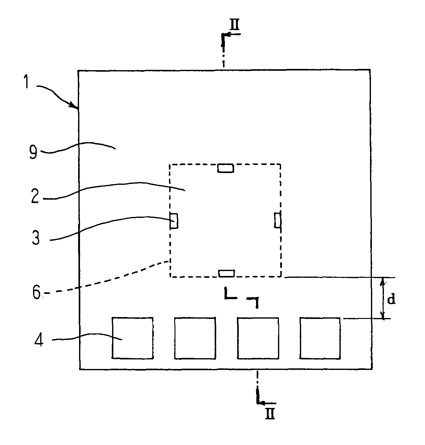
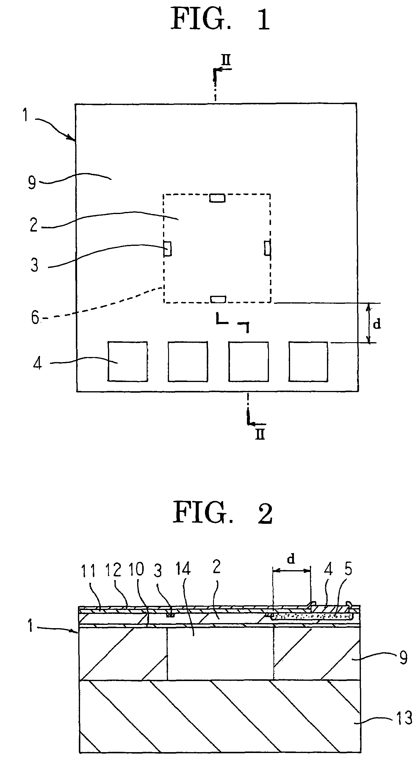
[0014]FIG. 1 is a plan that schematically shows a configuration of a semiconductor strain sensor according to Embodiment 1 of the present invention, and FIG. 2 is a cross section that is taken along line II-II in FIG. 1 so as to be viewed from the direction of the arrows. A semiconductor strain sensor according to Embodiment 1 is assumed to be for measuring intake air pressure inside an intake manifold of a vehicle engine, and to have a pressure range that is up to approximately 5 atmospheres.

[0015]In FIGS. 1 and 2, an SOI substrate 1 is prepared, for example, by fixing together two silicon substrates by means of an embedded oxide film 10, and polishing the silicon substrate on a front surface to a desired thickness. The SOI substrate 1 includes: a thin, pressure-detecting diaphragm portion 2; and a thick outer frame portion 9 that is formed around the diaphragm portion 2. The diaphragm portion 2 is formed by applying deep reactive ion etching (DRIE) from a rear surface of the SOI s...

embodiment 2

[0029]In Embodiment 2, electrodes 4 are disposed at positions on an outer frame portion 9 that are separated by greater than or equal to 120 μm toward the outer frame portion 9 from a boundary line between a diaphragm portion 2 and the outer frame portion 9.

[0030]Moreover, the rest of this embodiment is configured in a similar manner to Embodiment 1 above.

[0031]In semiconductor strain sensor manufacturing processes, there may be deviations in the processing precision of the diaphragm portion 2 and the electrodes 4. Positions at the boundary line 6 between the diaphragm portion 2 and the outer frame portion 9 in particular deviate easily since the diaphragm portion 2 is formed by etching from the rear surface of the SOI substrate 1 using DRIE.

[0032]Thus, if a lower limit of the distance d between the boundary line 6 between the diaphragm portion 2 and the outer frame portion 9 and the electrodes 4 is set to 100 μm, there is a risk that sensor chips in which the distance d is less tha...

embodiment 3

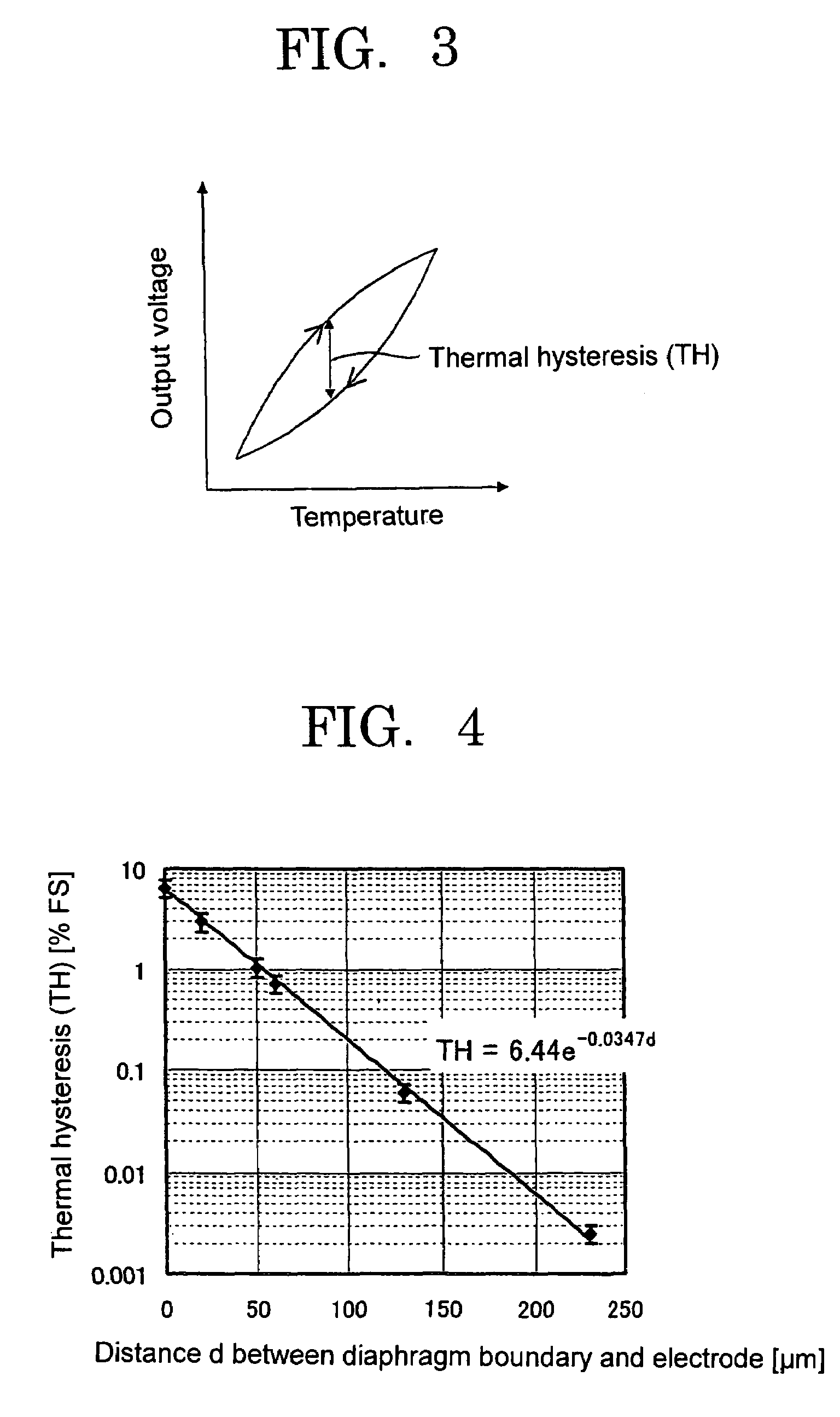
[0034]In Embodiment 3, thickness of a diaphragm portion 2 is stipulated as less than or equal to 30 μm.

[0035]Moreover, the rest of this embodiment is configured in a similar manner to Embodiment 1 above.

[0036]According to Embodiment 3, because the thickness of the diaphragm portion 2 is stipulated to be less than or equal to 30 μm, the effects of thermal stresses from the electrodes 4 on the piezoresistive elements 3 can be reduced, enabling thermal hysteresis of the output voltage per sensor chip unit to be reliably suppressed to less than or equal to 0.2 percent FS.

[0037]Here, considering sensor characteristics, it is desirable for the thickness of the diaphragm portion 2 to be set to greater than or equal to 1 μm.

[0038]Moreover, in each of the above embodiments, the semiconductor strain sensor is explained as being used in a pressure sensor, but the semiconductor strain sensor is not limited to pressure sensors and may also be used in other physical quantity sensors such as accel...


PUM


Abstract

An SOI substrate includes a thin diaphragm portion that is formed by removing a portion of the substrate from a rear surface side, and a thick outer frame portion that surrounds the diaphragm portion. A piezoresistive element that outputs an electrical signal in response to pressure is formed on the diaphragm portion, and an electrode that extracts the electrical signal from the piezoresistive element is formed on the outer frame portion. The electrode is disposed at a position on the outer frame portion that is separated by greater than or equal to 100 μm from a boundary line between the diaphragm portion and the outer frame portion.

Description

BACKGROUND OF THE INVENTION[0001]1. Field of the Invention[0002]The present invention relates to a semiconductor strain sensor that includes a piezoresistive element and an electrode for externally extracting a signal from the piezoresistive element on a silicon-on-insulator (SOI) substrate.[0003]2. Description of the Related Art[0004]Conventional semiconductor strain sensors include: a semiconductor substrate such as single-crystalline silicon, etc., in which are formed: a thin diaphragm portion; and a thick outer frame portion that is positioned around the diaphragm portion; and a glass pedestal that is joined to the outer frame portion of the semiconductor substrate (see Patent Literature 1, for example). A plurality of strain gauge resistors in which resistance changes due to piezoresistance effects when pressure is applied are disposed on the diaphragm portion so as to constitute a bridge circuit, and pressure is detected by detecting changes in the resistance of the strain gau...

Claims


Application Information

Patent Timeline
Patent Type & Authority Patents(United States)
IPC IPC(8): G01B7/16
CPCG01L19/04G01L9/0055H01L29/84
Inventor YOSHIKAWA, EIJITARUYA, MASAAKI
Owner MITSUBISHI ELECTRIC CORP
Why Eureka
Try Eureka