Layout printability optimization method and system

a printability optimization and printability technology, applied in the field oflayout printability optimization methods, can solve the problems of reducing pattern tolerance, lithographic process becoming increasingly difficult, optical pattern transfer process approaching fundamental resolution limits, etc., and achieves the effect of improving manufacturability and yield

Inactive Publication Date: 2009-07-28
KROYAN ARMEN +1
View PDF5 Cites 26 Cited by
  • Summary
  • Abstract
  • Description
  • Claims
  • Application Information

AI Technical Summary

Benefits of technology

[0014]The present invention seeks to provide a methodology, which contrary to the prior art, applies advanced nonlinear optimization techniques to solv...

Problems solved by technology

With the continuing shrinkage of the IC devices, the lithographic process has become increasingly challenging.
As circuit pattern dimensions became smaller than the wavelength of light used for their imaging, the optical pattern transfer process approached its fundamental resolution limits and became highly nonlinear.
Such problems include but are not limited polygon edge placement errors, pattern distortions, pattern fidelity (i.e. image contrast, slope) reduced pattern tolerance to process variations (i.e. exposure dose, focus, aberrations, etc.), and printability hot spots, which significantly reduce the yield of the integrated circuit.
However, as the imaging non-linearities and the proximity effects increased, rule-based OPC was no longer sufficient and became replaced by a model-based approach.
As the industry moved into the deep sub-100 nm technology space, new printability challenges emerged.
These hot spots have become one of the biggest limiting factors of the IC yield, and they threaten to become even more dominant of an issue as the industry moves into 45 nm technology and below.
The OPC technology alone cannot cope with this problem ...

Method used


Image

  • Layout printability optimization method and system
  • Layout printability optimization method and system
  • Layout printability optimization method and system

Examples


Embodiment Construction

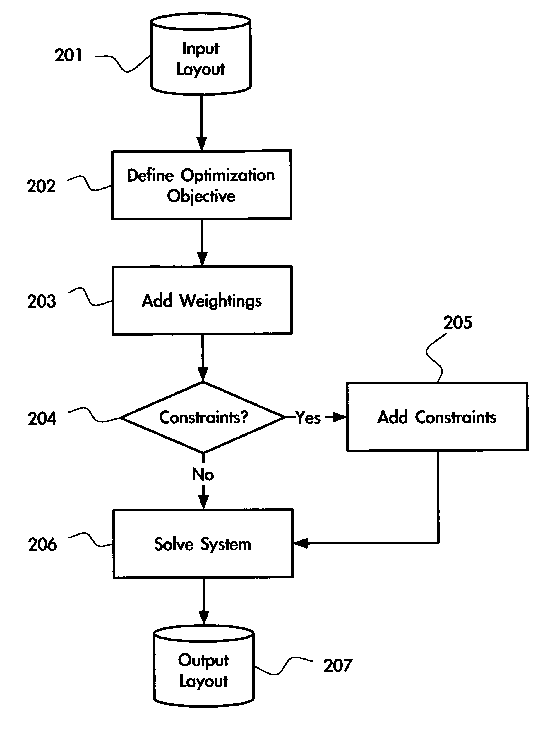
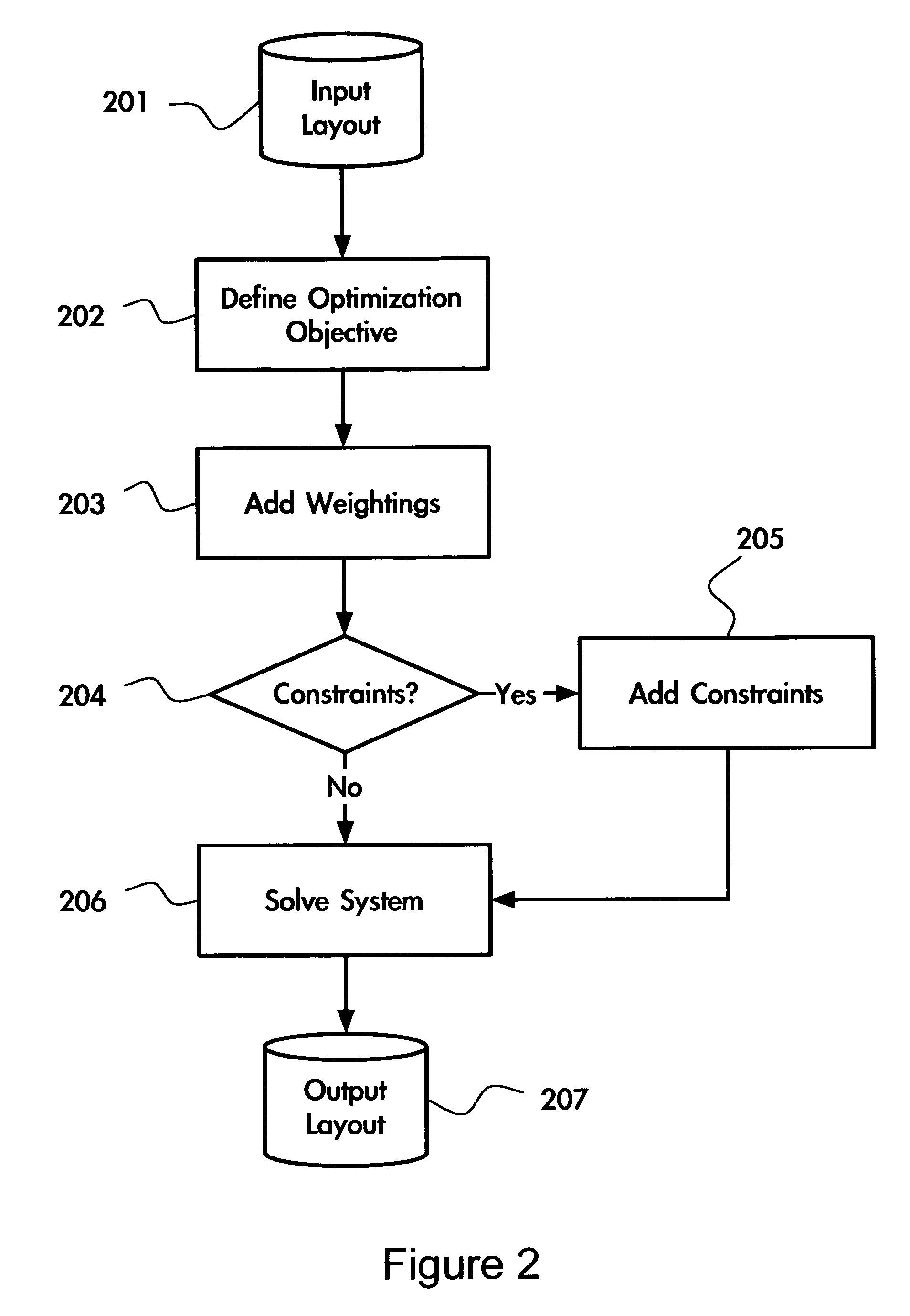
[0041]The layout printability optimization method and system, described in the present invention, may be applied to an IC physical layout data that is subsequently used in mask data preparation and generation processes. This optimization methodology is applicable to various resolution enhancement technologies (RETs) currently used in the state-of-the-art lithography. For example, this optimization methodology may be used for binary “chrome-on-glass” masks and phase shifting masks (i.e. attenuated, alternating-aperture). Moreover, this methodology is complimentary to sub-resolution assist feature (scattering bar) techniques, and may be applied to multiple exposure techniques based on layout decomposition. It is also contemplated that the optimization methodology and system described herein may take advantage of layout hierarchy information provided with the IC layout data, for faster and more efficient layout processing, and that the optimization methodology and system preserves the ...


PUM


Abstract

A layout printability optimization method and system is presented that may be used for enhancing the manufacturability and yield of integrated circuits. The method is based on a mathematical framework, which describes and solves layout printability problems using nonlinear numerical optimization techniques. The means to define an optimization objective, constraint functions, compute function derivatives, and solve the resulting system, are also presented.

Description

FIELD OF THE INVENTION[0001]The present invention relates to layout printability optimization methods implemented in software programs for improving the manufacturability and yield of semiconductor integrated circuits.BACKGROUND OF THE INVENTION[0002]The following U.S. Pat. Nos. 6,189,132, 6,473,882, 6,507,931, and 6,928,634 are believed to represent the current state of the art. These patents all relate to prior art with respect to the current patent.[0003]The above patents describe techniques to improve the printability of mask photolithography as it pertains to the manufacture of integrated circuits.[0004]Over the past several decades, integrated circuit (IC) manufacturing has been based on the optical pattern transfer process called photolithography. A completed IC design layout is captured in a form of multiple design layers corresponding to various processing steps involved in a formation of semiconductor devices in silicon. Each of the sequential processing steps requires a p...

Claims


Application Information

Patent Timeline
IPC IPC(8): G06F17/50
CPCG03F1/36G03F1/144
Inventor KROYAN, ARMENKROYAN, JULIA
Owner KROYAN ARMEN
Why Eureka
Try Eureka