

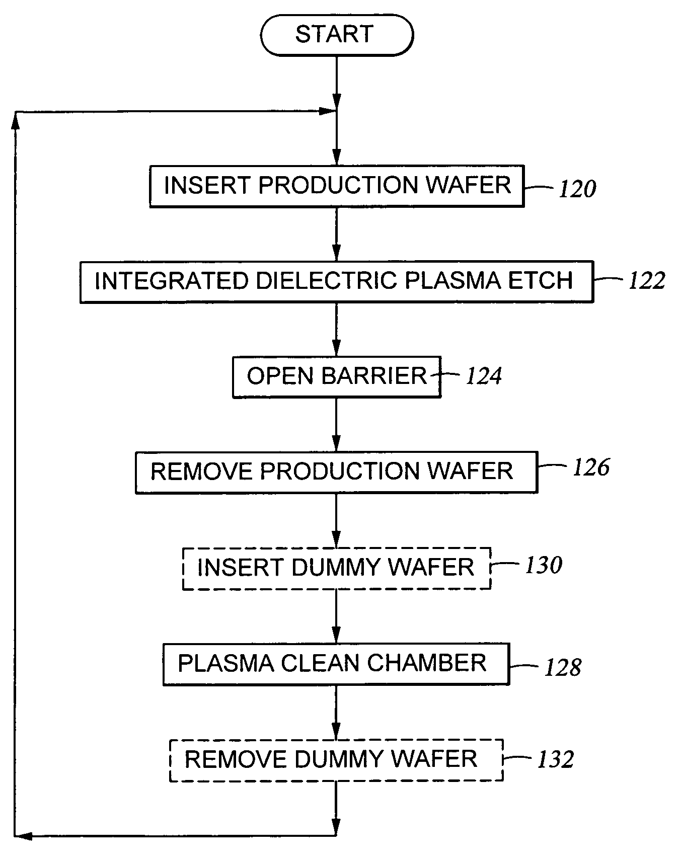
Chamber recovery after opening barrier over copper
a technology of opening barrier and chamber, which is applied in the direction of cleaning process and apparatus, chemistry apparatus and processes, electric discharge tubes, etc., can solve the problems of difficult cleaning of plasma etch chambers and difficulty in the remainder
- Summary
- Abstract
- Description
- Claims
- Application Information
AI Technical Summary
Benefits of technology
Problems solved by technology
Method used
Image

Examples
Embodiment Construction
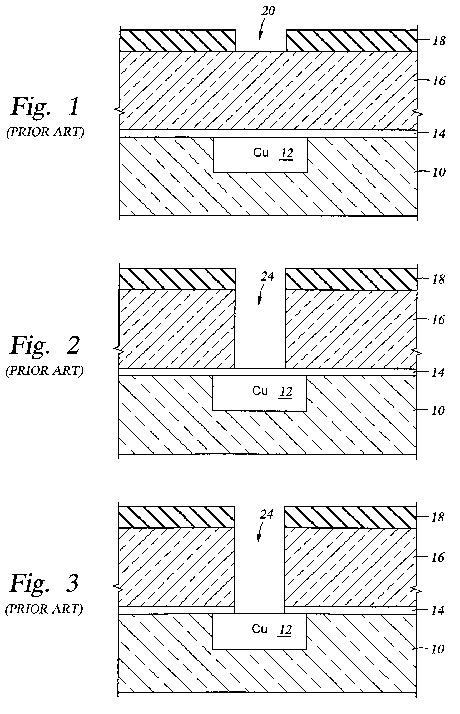
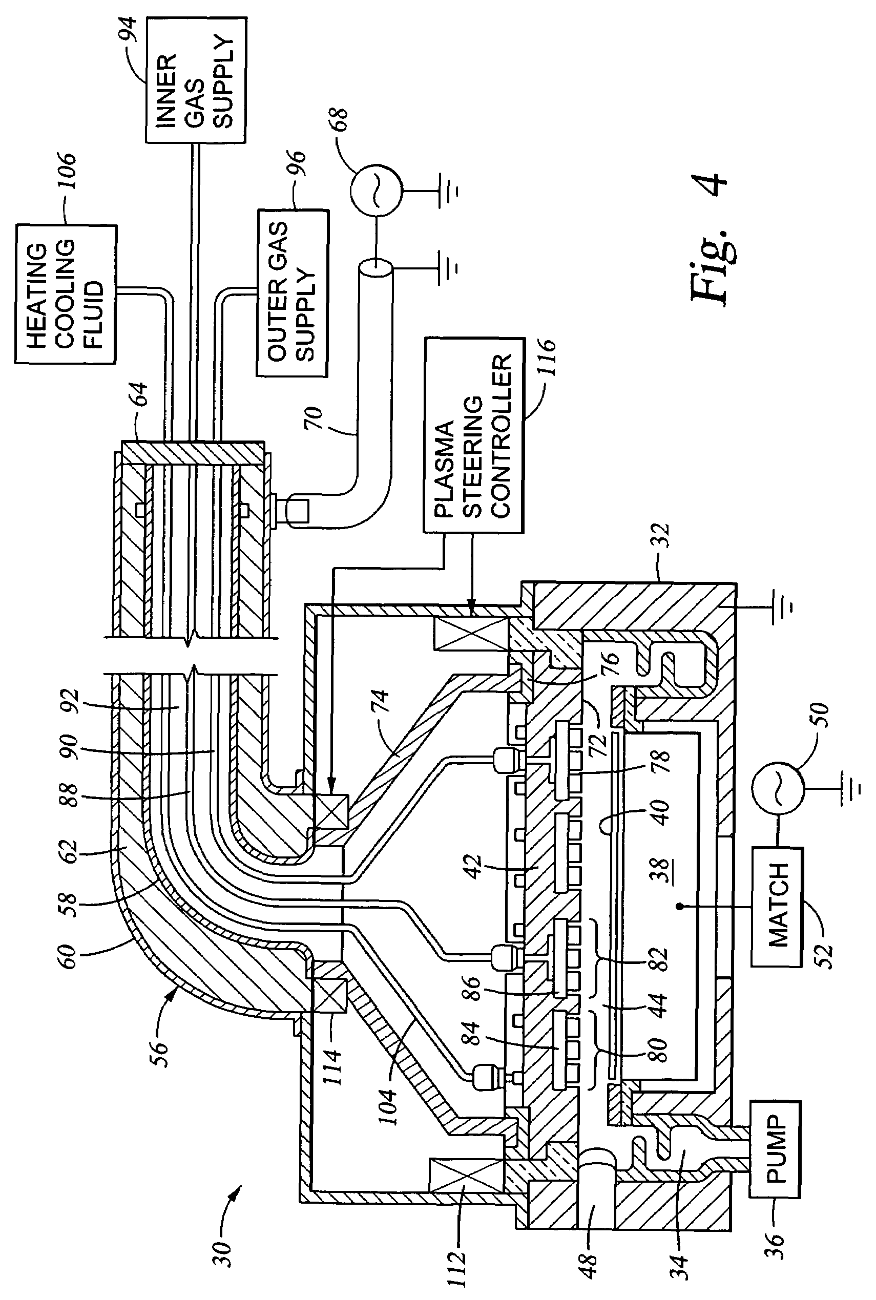
[0024]We have observed that an integrated dielectric etch process for inter-level connect structures performed in a capacitively coupled etch chamber sometimes experiences a problem of chamber contamination caused by sputtering copper in the barrier open step. Opening the barrier necessarily exposes the underlying copper to the barrier etching environment. As always, some amount of over etching of the barrier is required to assure that all the barrier material is removed from over the entire wafer and in spite of any process drift. However, barrier materials are necessarily relatively rugged and difficult to etch. Removal of the barrier layer seems to necessitate reactive ion etching with ion energies of at least 20 eV. Such high ion energies will also sputter copper atoms from the relatively soft underlying copper contact 12 of FIG. 3 exposed at the end of the barrier open. We have observed that copper is coated onto parts of the plasma etch chamber 30 of FIG. 4, for example, the s...
PUM
| Property | Measurement | Unit |
|---|---|---|
| HF frequency | aaaaa | aaaaa |
| HF frequency | aaaaa | aaaaa |
| diameter | aaaaa | aaaaa |
Abstract
Description
Claims
Application Information