

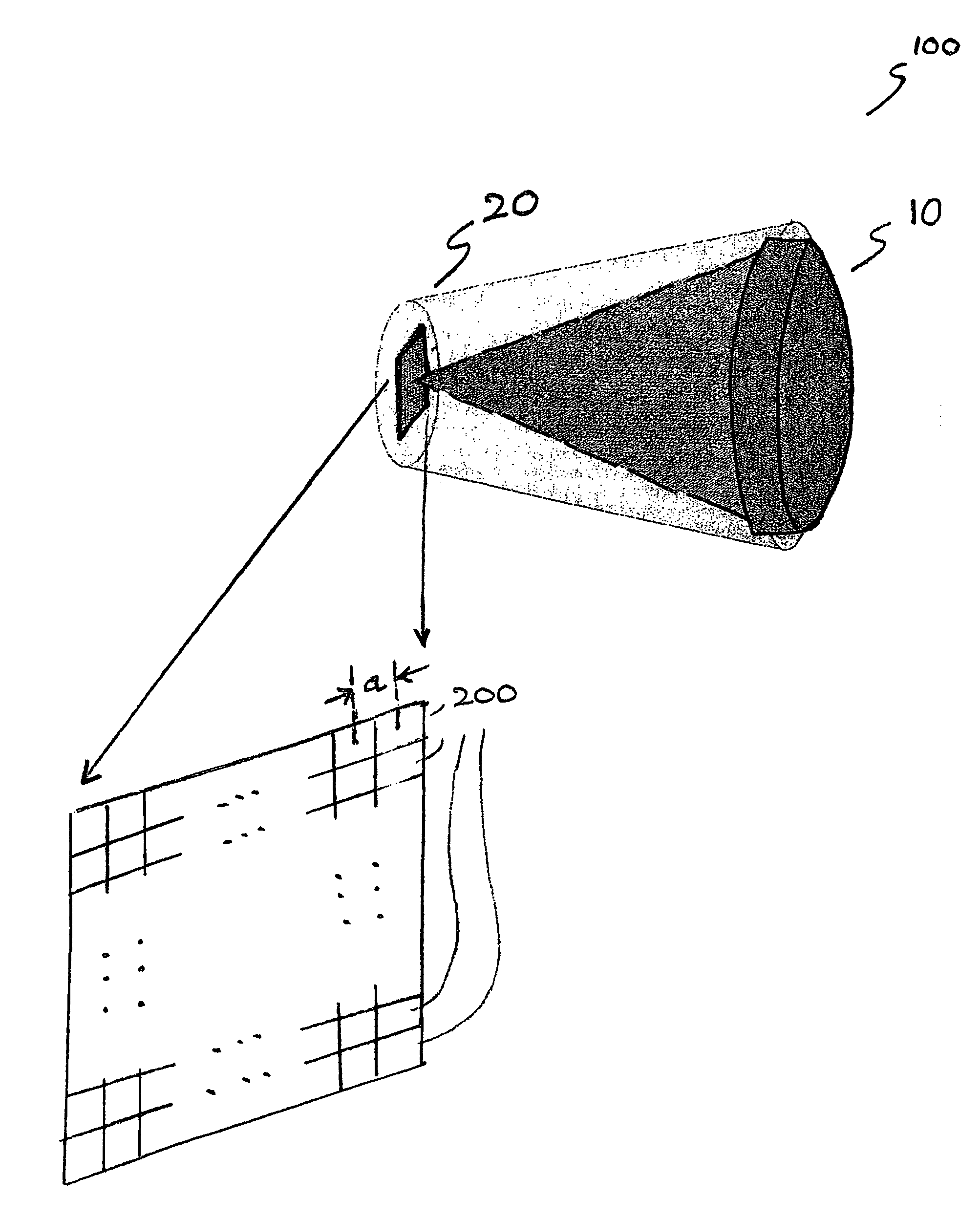
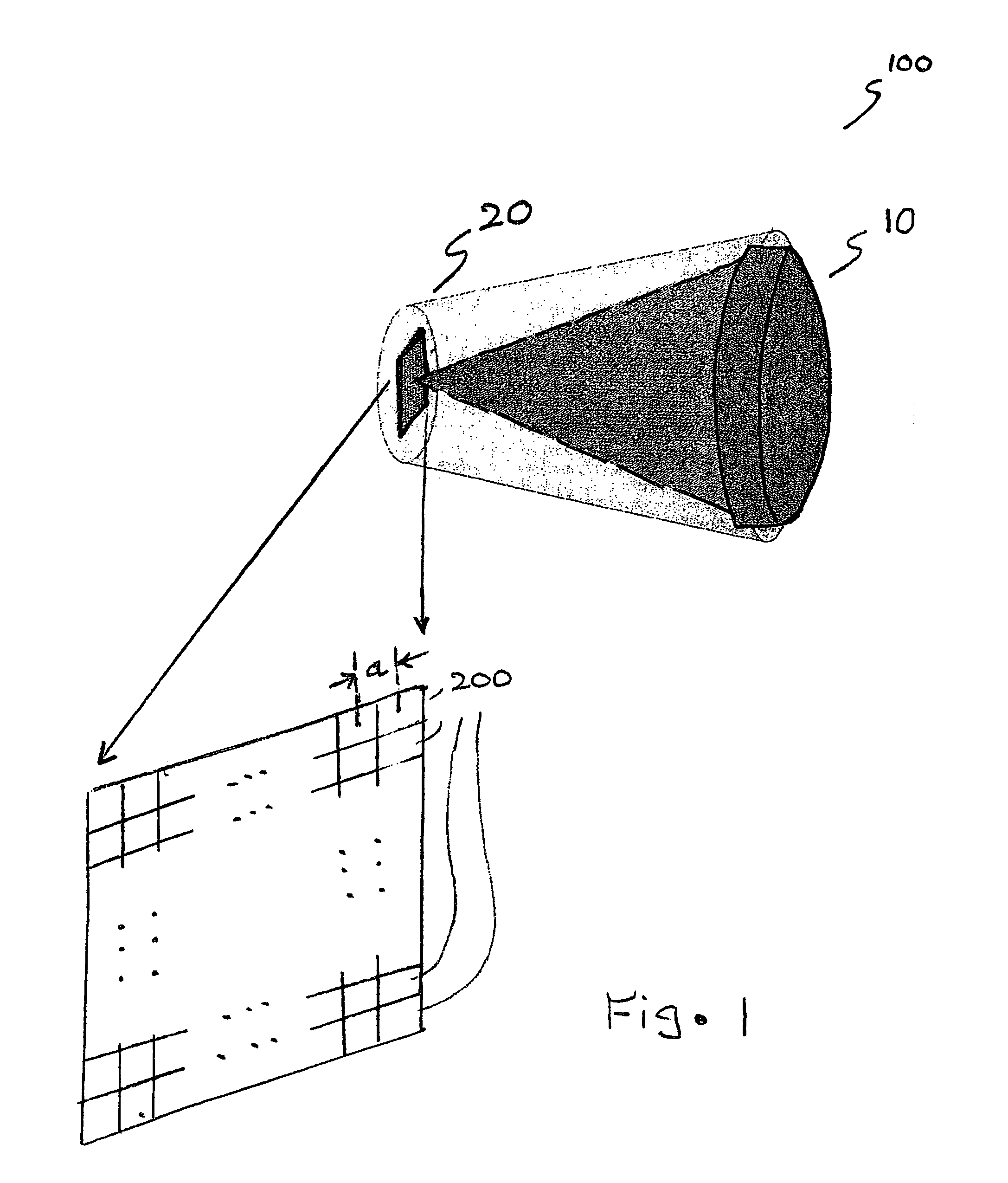
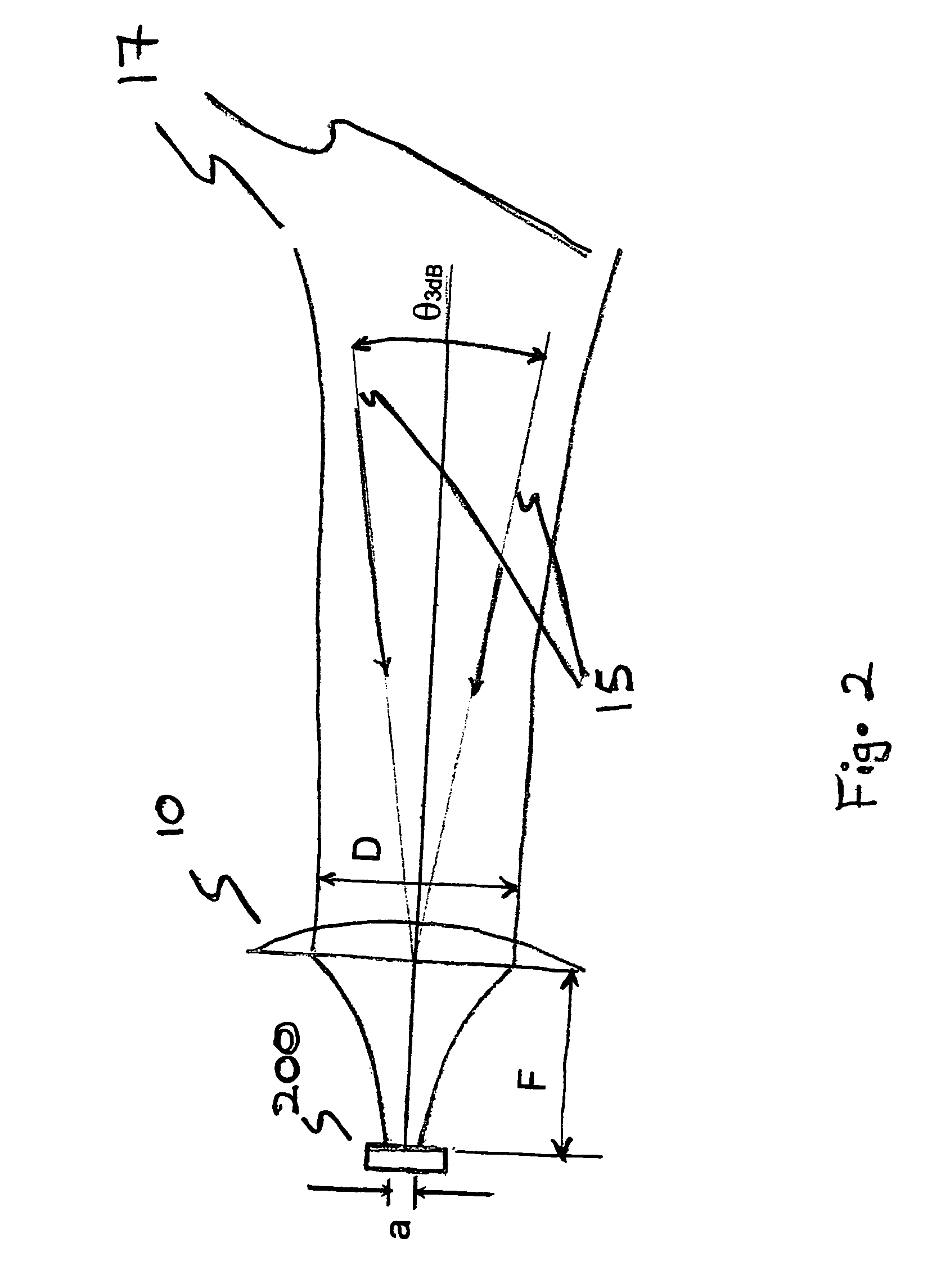
Low cost millimeter wave imager
a millimeter wave and imager technology, applied in the field of millimeter wave imaging systems, can solve the problems of high sensor cost, low noise, and other detectors that do not provide the responsivity, including schottky diodes, and achieve low cost and useful sensitivity levels.
- Summary
- Abstract
- Description
- Claims
- Application Information
AI Technical Summary
Benefits of technology
Problems solved by technology
Method used
Image

Examples
Embodiment Construction
[0035]In accordance with the present invention detectors based upon a BTD as taught in U.S. Pat. No. 6,635,907, the entire content of which is incorporated herein by reference, are integrated with a low noise antenna array and readout electronics, resulting in a low cost imager.
[0036]A BTD is a high-speed semiconductor device that exhibits an interband tunneling characteristic. Two semiconductor regions that have different compositions from one another are separated by a thin interface layer. The two semiconductor regions have energy bands shifted in opposite directions and the interface layer is thin in order to allow for electron transfer through tunneling. The BTD typically includes a heterostructure of a first layer of InAs and a second layer of GaSb or InGaSb with an interface layer of an aluminum antimonide compound. The presence of aluminum antimonide compound in the interface enhances the highly nonlinear current-voltage (I-V) curve near zero bias.
[0037]The band gap engineer...
PUM
 Abstract
Description
Claims
Application Information