Rare earth element-doped oxide precursor with silicon nanocrystals

a technology of rare earth elements and precursors, applied in semiconductor/solid-state device manufacturing, basic electric elements, electric devices, etc., can solve the problems of low device efficiency, increased cost, and insufficient interface engineering to support the use of rare earth element-doped oxide precursors, etc., to achieve the effect of reducing production costs

Inactive Publication Date: 2009-09-08
SHARP KK
View PDF1 Cites 3 Cited by
  • Summary
  • Abstract
  • Description
  • Claims
  • Application Information

AI Technical Summary

Benefits of technology

[0009]Described herein is an economical procedure to form a precursor that can be used to deposit a film comprised of silicon oxide with a large number of nanocrystalline silicon particles, having a size of about 10 to 30 Å, with rare earth doping. In contrast to the conventional method of Si implantation to form nc-Si, the present invention process can be scaled to larger substrates with a lower cost of production.
[0010]The invention employs a chemical synthesis process to obtain the nc-Si layer with rare earth element doping, as opposed to a process that forms an SRO layer using ion implantation, followed by another implantation for rare earth doping. In contrast, the present invention synthesizes Si nanoclusters, followed by the incorporation of the nc Si particles with rare earth elements in a precursor solution. The rare earth doped nc-Si layer can then be formed by a spin-coating technique. The benefit of this process method is better control of the nc Si concentration in the SRO layer, lower cost, and the direct attachment of rare earth elements on the nc Si particle surface.

Problems solved by technology

However, state-of-the-art implantation processes have not been able to distribute the dopant uniformly, which lowers the light emitting efficiency and increases costs.
At the same time, there has been no interface engineering sufficient to support the use of such a dopant.
The device efficiency is very low and the process temperature is very high, which limits the device applications.
Silicon has conventionally been considered unsuitable for optoelectronic applications, due to the indirect nature of its energy band gap.
Bulk silicon is indeed a highly inefficient light emitter.
However as mentioned above, the device efficiency is very low and the process temperature is very high, normally over 1100° C.
That is, the making of a large area of Si—SiO2 interface is a critical issue for EL device applications.

Method used


Image

  • Rare earth element-doped oxide precursor with silicon nanocrystals
  • Rare earth element-doped oxide precursor with silicon nanocrystals
  • Rare earth element-doped oxide precursor with silicon nanocrystals

Examples


Embodiment Construction

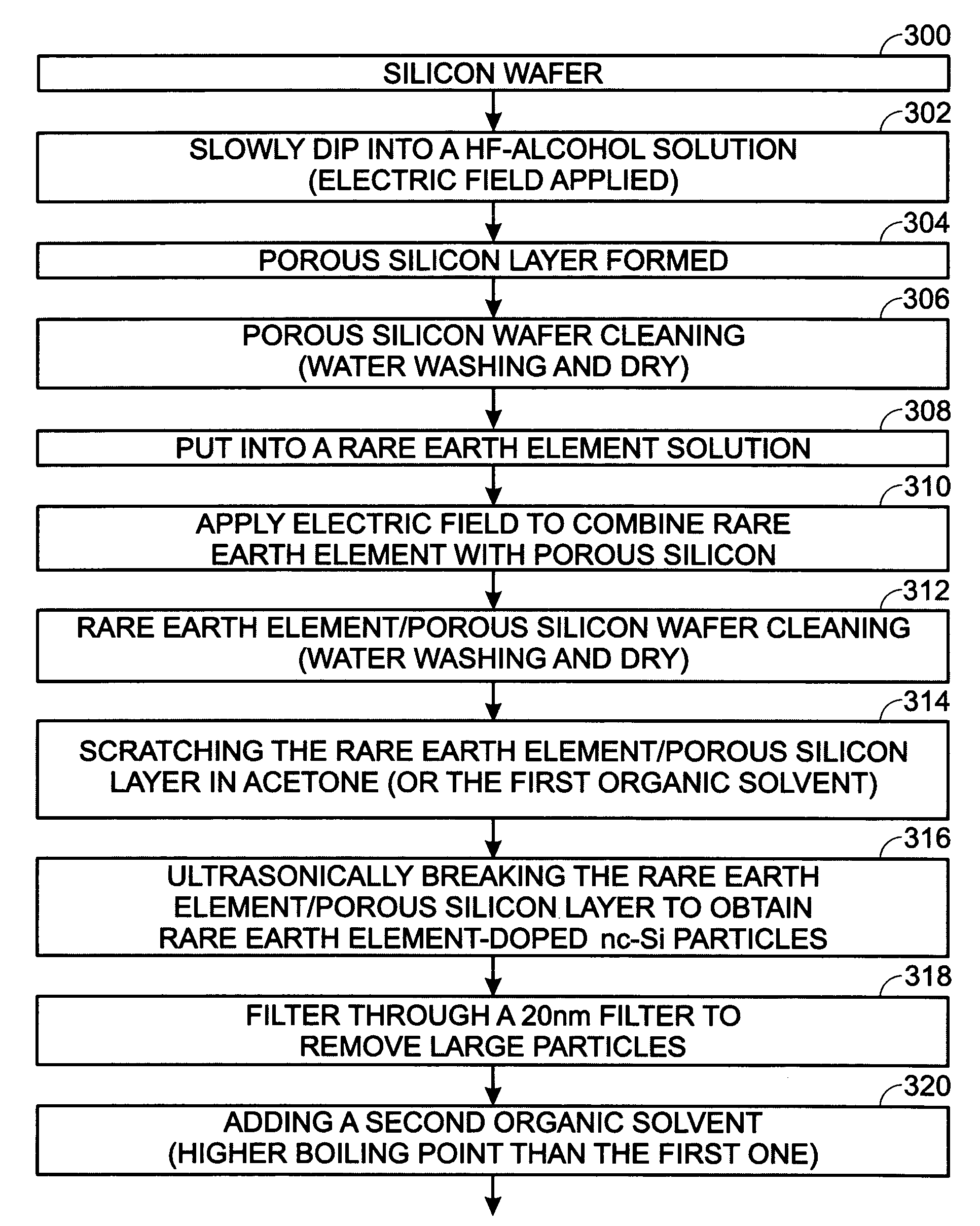
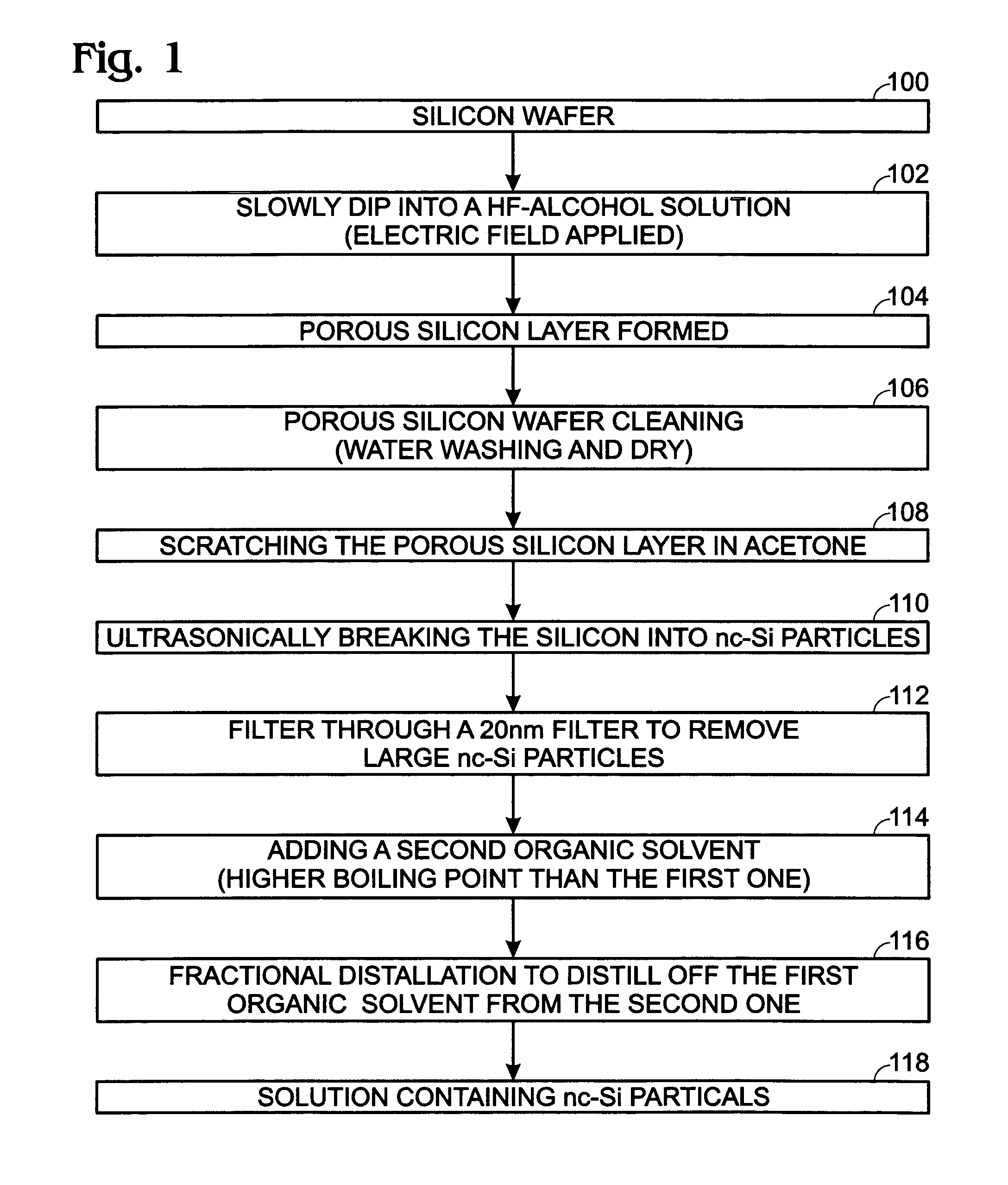
[0022]FIG. 1 is a diagram depicting a process for forming a nc Si solution. The synthesis of nc Si particles includes four basic steps. In the first basic step (Steps 100-108), a porous silicon layer is formed through an electrochemical etch process. The solution for the electrochemical process is the mixture of HF( about 49%) and alcohol, such as the methanol or ethanol. The porous silicon layer is formed by slowly immersing the wafer into the solution while keeping an electrical bias on the wafer. The thickness of the resulting porous silicon layer depends on the immersion speed, current density, solution concentration, and wafer properties.

[0023]The second step (Step 110) is the transfer of the porous silicon layer into an organic solvent. An ultrasonic treatment can be used in the step to separate the porous silicon layer from the wafer. The solvents used in this step include a strong polar organic solvent, such as acetone or tetrahydrofuran.

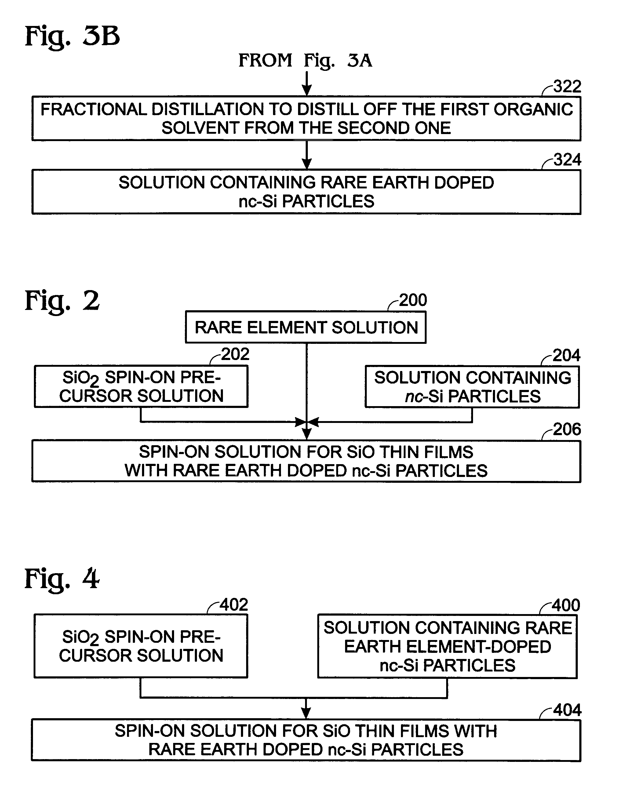
[0024]After transfer, the nc Si parti...


PUM

PropertyMeasurementUnit
temperatureaaaaaaaaaa
external quantum efficiencyaaaaaaaaaa
boiling pointaaaaaaaaaa

Abstract

A method is provided for forming a rare earth element-doped silicon oxide (SiO2) precursor with nanocrystalline (nc) Si particles. In one aspect the method comprises: mixing Si particles into a first organic solvent, forming a first solution with a first boiling point; filtering the first solution to remove large Si particles; mixing a second organic solvent having a second boiling point, higher than the first boiling point, to the filtered first solution; and, fractionally distilling, forming a second solution of nc Si particles. The Si particles are formed by immersing a Si wafer into a third solution including hydrofluoric (HF) acid and alcohol, applying an electric bias, and forming a porous Si layer overlying the Si wafer. Then, the Si particles are mixed into the organic solvent by depositing the Si wafer into the first organic solvent, and ultrasonically removing the porous Si layer from the Si wafer.

Description

RELATED APPLICATIONS[0001]The application is a continuation-in-part of a application entitled RARE EARTH ELEMENT-DOPED SILICON / SILICON DIOXIDE LATTICE STRUCTURE, invented by Li et al, Ser. No. 11 / 039,463, filed on Jan. 19, 2005 and issued as U.S. Pat. No. 7,256,426, which is incorporated herein by reference.BACKGROUND OF THE INVENTION[0002]1. Field of the Invention[0003]This invention generally relates to integrated circuit (IC) fabrication and, more particularly, to a procedure for making a rare earth element-doped silicon oxide (SiO2) precursor with nanocrystalline (nc) Si particles, for use in silicon-based electroluminescence (EL) devices.[0004]2. Description of the Related Art[0005]The observation of visible luminescence at room temperature, emanating from porous silicon (Si), has spurred a tremendous amount of research into using nano-sized Si to develop a Si-based light source. One widely used method of fabricating nanocluster Si (nc-Si) is to precipitate the nc-Si out of SiO...

Claims


Application Information

Patent Timeline
Patent Type & Authority Patents(United States)
IPC IPC(8): H01L21/31
CPCH01L21/316H01L21/02156H01L21/02282
Inventor ZHUANG, WEI-WEIONO, YOSHIHSU, SHENG TENGLI, TINGKAI
Owner SHARP KK
Why Eureka
Try Eureka