Semiconductor device including active layer of zinc oxide with controlled crystal lattice spacing and manufacturing method thereof

a technology of zinc oxide and active layer, which is applied in the direction of semiconductor devices, semiconductor/solid-state device details, electrical devices, etc., can solve the problems of desorption of zinc or oxygen from defects in the oxide semiconductor thin film layer, and the inability to disclose the method, etc., to achieve excellent performance

Inactive Publication Date: 2009-10-06
KOICHI IND PROMOTION CENT +1
View PDF3 Cites 209 Cited by
  • Summary
  • Abstract
  • Description
  • Claims
  • Application Information

AI Technical Summary

Benefits of technology

[0016]One object of the present invention is to provide a semiconductor device that includes an oxide semiconductor thin film layer of zinc oxide and that exhibits excellent performance even after being subjected to a heat treatment process during formation of an insulating film or the like.

Problems solved by technology

However, this publication does not disclose how the physical properties (e.g., orientation and lattice constant) of zinc oxide affect the heat resistance of the zinc oxide or the performance of semiconductor devices which include a TFT or the like.
Since zinc oxide has a poor heat resistance, the heat history during the protective insulator formation results in desorption of zinc or oxygen from the oxide semiconductor thin film layer as well as defects in the oxide semiconductor thin film layer.
The defects form a shallow impurity level and reduce the resistance of the oxide semiconductor thin film layer.
The defects formed on the back channel side greatly affect the performance of the bottom gate TFT.

Method used


Image

  • Semiconductor device including active layer of zinc oxide with controlled crystal lattice spacing and manufacturing method thereof
  • Semiconductor device including active layer of zinc oxide with controlled crystal lattice spacing and manufacturing method thereof
  • Semiconductor device including active layer of zinc oxide with controlled crystal lattice spacing and manufacturing method thereof

Examples


first embodiment

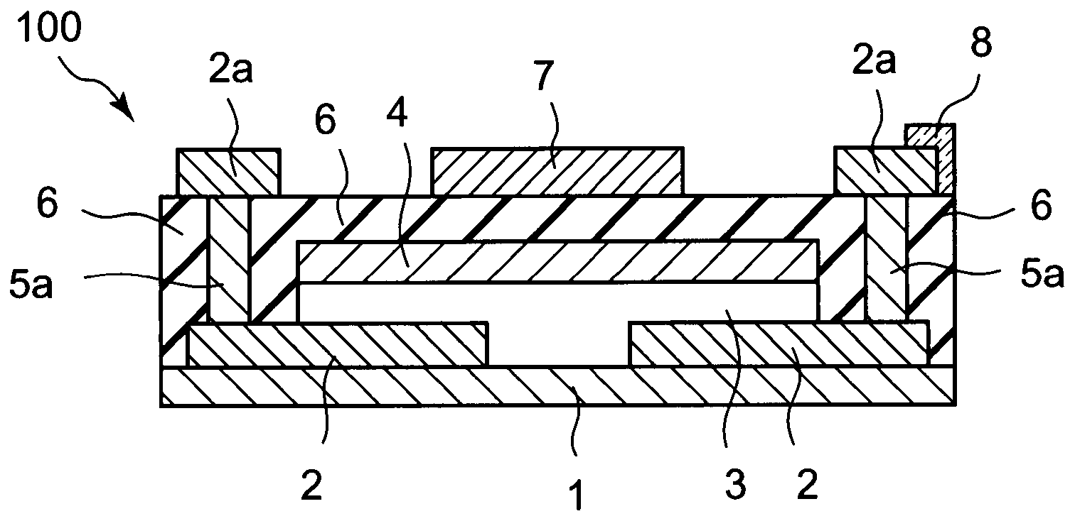
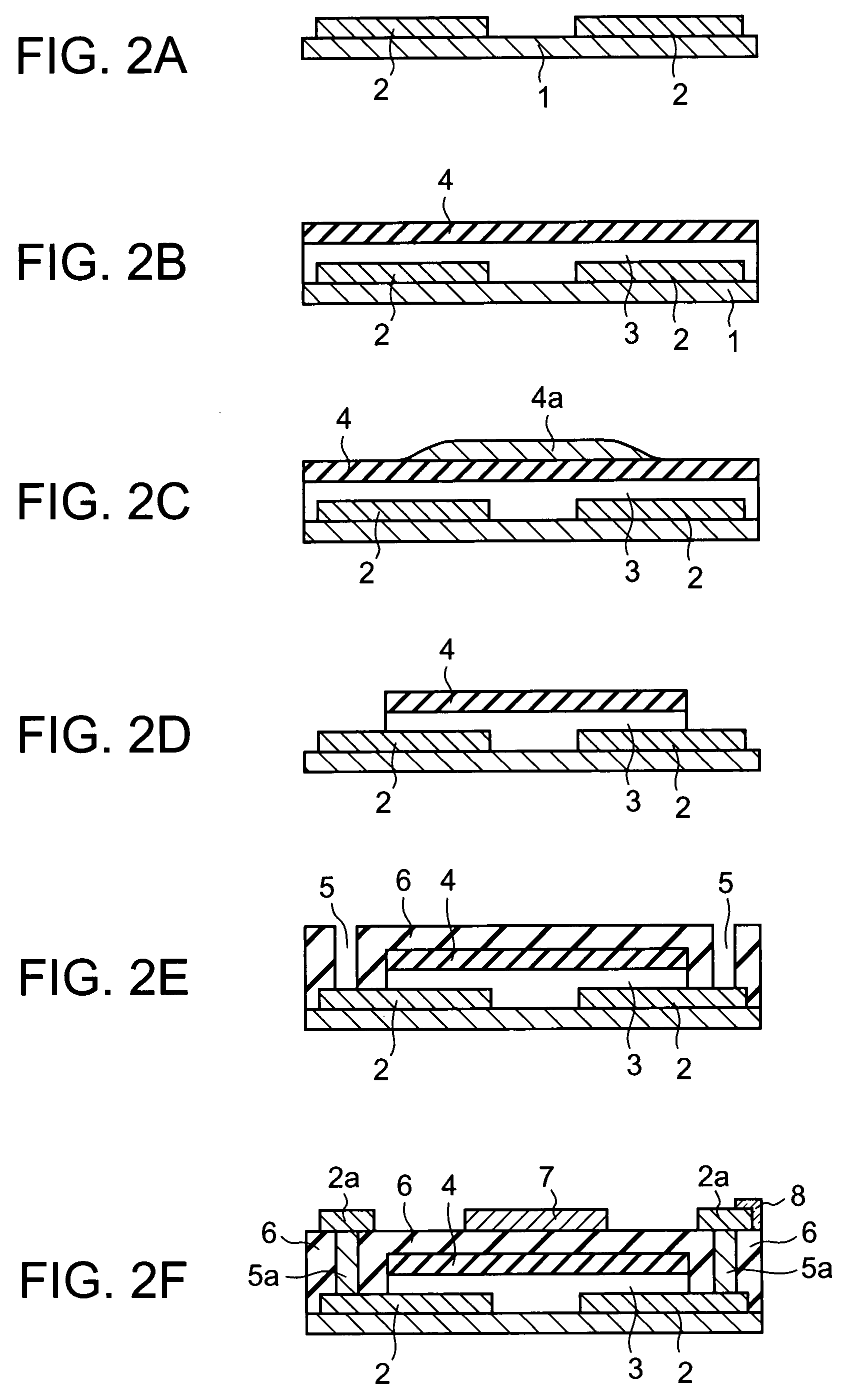
[0039]FIG. 1 shows the structure of a thin film transistor 100 according to the first embodiment of the present invention. Thin film transistor 100, which has a top-gate structure, is supported on substrate 1, and includes: a pair of source / drain electrodes 2, an oxide semiconductor thin film layer 3, a first gate insulator 4, contact parts 5a, a pair of external source / drain electrodes 2a, a second gate insulator 6, a gate electrode 7, and a display electrode 8.

[0040]The pair of source / drain electrodes 2 are formed on substrate 1. Source / drain electrodes 2 are spaced apart from each other on the upper surface of substrate 1.

[0041]Oxide semiconductor thin film layer 3 is formed on substrate 1 and the pair of source / drain electrodes 2. Oxide semiconductor thin film layer 3 is arranged such that a channel is formed between a source electrode and a drain electrode of source / drain electrodes 2. Oxide semiconductor thin film layer 3 is formed by an oxide semiconductor mainly comprising z...

second embodiment

[0067]Next, a thin film transistor 200 according to the second embodiment of the present invention will be described. In the following description, parts that are similar to or the same as parts described above with respect to the thin film transistor 100 of the first embodiment will be identified with the same reference numerals as used above with respect to the thin film transistor 100 according to the first embodiment, and description of these parts will be omitted.

[0068]FIG. 3 shows a cross section of thin film transistor 200 according to the second embodiment of the present invention. Thin film transistor 200 is formed on a substrate 1, and includes: a pair of source / drain electrodes 2, a pair of contact layers 10, an oxide semiconductor thin film layer 3, a first gate insulator 4, contact parts 5a, a pair of external source / drain electrodes 2a, a second gate insulator 6, a gate electrode 7, and a display electrode 8. These layers are combined in this order as shown in FIG. 3. ...

sixth embodiments

Third to Sixth Embodiments

[0094]Next, thin film transistors according to the third to sixth embodiments of the present invention will be described.

[0095]Oxide semiconductor thin film layer 3 of the thin film transistors according to the third to sixth embodiments includes a first region of intrinsic zinc oxide and second regions doped with donor ions. The first region is a channel region of the oxide semiconductor thin film layer 3 and the second regions are included in a pair of source / drain regions that define the channel region therebetween. The term “intrinsic zinc oxide” as used herein refers to zinc oxide that contains substantially no impurities. The term “dope” as used herein refers to a process of introducing ions and includes an ion-implantation process.


PUM


Abstract

A semiconductor device includes an oxide semiconductor thin film layer of zinc oxide. The (002) lattice planes of at least a part of the oxide semiconductor thin film layer have a preferred orientation along a direction perpendicular to a substrate of the semiconductor device and a lattice spacing d002 of at least 2.619Å.

Description

CROSS-REFERENCE TO RELATED APPLICATIONS[0001]This application is based upon and claims the benefit of priority from the prior Japanese Patent Applications No. 2006-155188 (filed on Jun. 2, 2006), No. 2006-155189 (filed on Jun. 2, 2006), and No. 2007-37176 (filed on Feb. 16, 2007), the entire contents of which are incorporated herein by reference.BACKGROUND OF THE INVENTION[0002]1. Field of the Invention[0003]The present invention relates to a semiconductor device including an active layer of zinc oxide with a controlled crystal lattice spacing and a manufacturing method thereof.[0004]2. Description of the Background Art[0005]It has been known for many years that zinc oxide has excellent characteristics as a semiconductor (an active layer). In recent years, active research and development of a semiconductor thin film layer of zinc oxide have been made in order to apply such a semiconductor thin film layer to a semiconductor device which includes a thin film transistor (hereinafter ab...

Claims


Application Information

Patent Timeline
Patent Type & Authority Patents(United States)
IPC IPC(8): H01L29/12H01L23/62H01L27/15H01L31/0256
CPCH01L29/78618H01L29/7869H01L29/04H01L29/045H01L29/458
Inventor HIRAO, TAKASHIHIRAMATSU, TAKAHIROFURUTA, MAMORUFURUTA, HIROSHIMATSUDA, TOKIYOSHI
Owner KOICHI IND PROMOTION CENT
Why Eureka
Try Eureka