
High brightness-multiple beamlets source for patterned X-ray production

a patterned x-ray and beamlet technology, applied in the field of high brightness and multiple beamlet xray sources, can solve the problems of low throughput, prohibitive throughput, and the insufficientness of optical lithography for the needs of the semiconductor industry, so as to improve focusing, reduce aberration, and improve the effect of focusing

Inactive Publication Date: 2009-10-27
RGT UNIV OF CALIFORNIA
View PDF8 Cites 11 Cited by
  • Summary
  • Abstract
  • Description
  • Claims
  • Application Information

AI Technical Summary

Benefits of technology

This patent describes a method and device for extracting patterned beamlets from a plasma source. The method involves using an extractor electrode with a plurality of apertures that pass through a conductive plasma side and an insulator, and a conductive exit side. The extractor electrode has one or more of the apertures connected to the conductive exit side. The method involves controllably biasing the conductive exit side of the apertures to extract a pattern of beamlets. The device includes a multicusp ion source with a plasma, computer controlled means for selectably extracting patterns of beamlets, and a target for impinging the beamlets to produce X-rays. The device can also include a detector for detecting X-ray transmission and scatter, and a computer for analyzing the data and providing a computed axial tomograph (CAT) scan. The technical effects of this patent include improved focusing and reduced aberrations in beamlet extraction, as well as improved accuracy and efficiency in ion implantation and maskless photolithography.

Problems solved by technology

As the dimensions of semiconductor devices are scaled down in order to achieve ever higher level of integration, optical lithography will no longer be sufficient for the needs of the semiconductor industry.
Significant challenges exist today for each of these techniques: for X-ray, EUV, and projection ion-beam lithography, there are issues with complicated mask technology; for e-beam and AFM lithography, there are issues with low throughput.
Focused ion beam (FIB) patterning of films is a well-established technique (e.g. for mask repair), but throughput has historically been a prohibitive issue in its application to lithographic processes in semiconductor manufacturing.
For the extraction of ions from a plasma source using a long, narrow channel, aberration is always a problem because of the edge effect.
Additional remaining problems in the semiconductor field relate to the manufacture of masks, changing of masks, and registration of masks.
These security measures, however, were not designed for scenarios in which individuals appear in an open environment and a security decision must be made at a distance from a suspected explosive.
The difficulty of the standoff explosive detection task is exacerbated by several factors, including dynamic backgrounds that can interfere with the signal from the explosive, the potential for high false alarms, and the need to ascertain a threat quickly so that action can be taken [1]
This background is also often dynamic, so that exemplary performance in controlled laboratory settings may be quite poor performance when applied in the field.

Method used


Image

  • High brightness-multiple beamlets source for patterned X-ray production
  • High brightness-multiple beamlets source for patterned X-ray production
  • High brightness-multiple beamlets source for patterned X-ray production

Examples


Embodiment Construction

Definitions

[0051]DC means direct current.

[0052]RF means radio frequency.

[0053]Coded means programmable, selectable, or programmable, such that in an electrode array may be selectably addressed at the one pixel or group of pixels level for patterned operation. Pixels may be simultaneously or sequentially addressed as needed for a given application.

[0054]μm means micron, or 10−6 meters.

Introduction

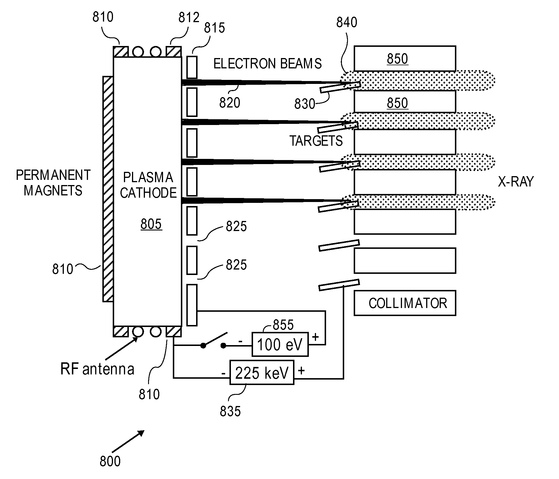
[0055]This application discusses methods of generation of multiple electron beamlets. Such system may be used in the generation of ion beamlets by suitable modification of the plasma source and extraction voltages. High brightness electron beamlets may strike an X-ray generating target to in turn produce high brightness X-ray sources. These X-ray sources may be collimated, or act as point sources with spherical radiation patters.

[0056]By a suitable choice of source plasma, ions may be extracted in high brightness beamlets to impinge on a target such as Ti to produce neutrons or gammas as des...


PUM


Abstract

Techniques for controllably directing beamlets to a target substrate are disclosed. The beamlets may be either positive ions or electrons. It has been shown that beamlets may be produced with a diameter of 1 μm, with inter-aperture spacings of 12 μm. An array of such beamlets, may be used for maskless lithography. By step-wise movement of the beamlets relative to the target substrate, individual devices may be directly e-beam written. Ion beams may be directly written as well. Due to the high brightness of the beamlets from extraction from a multicusp source, exposure times for lithographic exposure are thought to be minimized. Alternatively, the beamlets may be electrons striking a high Z material for X-ray production, thereafter collimated to provide patterned X-ray exposures such as those used in CAT scans. Such a device may be used for remote detection of explosives.

Description

CROSS REFERENCE TO RELATED APPLICATIONS[0001]This patent application claims benefit of priority to U.S. Provisional patent application 60 / 803,671 filed Jun. 1, 2006, entitled “High Brightness and Multiple Beamlets Source for Maskless Lithography”, which is hereby incorporated by reference in its entirety.STATEMENT REGARDING FEDERAL FUNDING[0002]This invention was made with U.S. Government support under Contract Number DE-AC02-05CH11231 between the U.S. Department of Energy and The Regents of the University of California for the management and operation of the Lawrence Berkeley National Laboratory. The U.S. Government has certain rights in this invention.REFERENCE TO A COMPUTER PROGRAM[0003]Not Applicable.BACKGROUND OF THE INVENTION[0004]1. Field of the Invention[0005]The present invention relates generally to a high brightness and multiple beamlets X-ray source, more specifically to a high brightness and multiple beamlets X-ray source for patterned particle generation, and most spec...

Claims


Application Information

Patent Timeline
Patent Type & Authority Patents(United States)
IPC IPC(8): H01J35/06
CPCB82Y10/00G01N23/203G01V5/0008H01J3/025H01J3/04H01J27/024H01J35/00H01J37/045H01J37/077H01J37/08H01J37/3172H01J37/3174H01J37/3177B82Y40/00H01J2237/3171H01J2235/06H01J2235/068H01J2237/0435H01J2237/061H01J2237/06366H01J2237/06375G01V5/20
Inventor LEUNG, KA-NGOJI, QINGBARLETTA, WILLIAM A.JIANG, XIMANJI, LILI
Owner RGT UNIV OF CALIFORNIA
Learn More