High performance transistors with hybrid crystal orientations

a technology of hybrid crystals and transistors, applied in the field of metal oxide semiconductor field effect transistors (mosfets), can solve the problems of inability to adapt to nfet devices, significant deformation of electron mobilities on (110) si surfaces, and undesirable width of pfets, etc., and achieves less complex fabrication processes and more scalable effects

Inactive Publication Date: 2009-11-03
TAIWAN SEMICON MFG CO LTD +1
View PDF28 Cites 7 Cited by
  • Summary
  • Abstract
  • Description
  • Claims
  • Application Information

AI Technical Summary

Benefits of technology

[0011]A method of forming a semiconductor structure having a hybrid crystal orientation and forming MOSFETs having improved performance is provided.
[0015]By using preferred embodiments of the present invention, the semiconductor devices are more scalable, and the fabrication processes are less complex.

Problems solved by technology

PFETs having greater widths are undesirable since they occupy a relatively greater amount of chip area.
Unfortunately, electron mobilities on (110) Si surfaces are significantly degraded compared to (100) Si surfaces.
As can be deduced from the above, the (110) Si surface is optimal for PFET devices because of excellent hole mobility, yet such a crystal orientation is inappropriate for NFET devices.
However, the method suffers drawbacks.
This posts a challenge for the simultaneous etching process and subsequent chemical mechanical polish for planarizing surfaces.

Method used


Image

  • High performance transistors with hybrid crystal orientations
  • High performance transistors with hybrid crystal orientations
  • High performance transistors with hybrid crystal orientations

Examples


Embodiment Construction

[0020]The making and using of the presently preferred embodiments are discussed in detail below. It should be appreciated, however, that the present invention provides many applicable inventive concepts that can be embodied in a wide variety of specific contexts. The specific embodiments discussed are merely illustrative of specific ways to make and use the invention, and do not limit the scope of the invention.

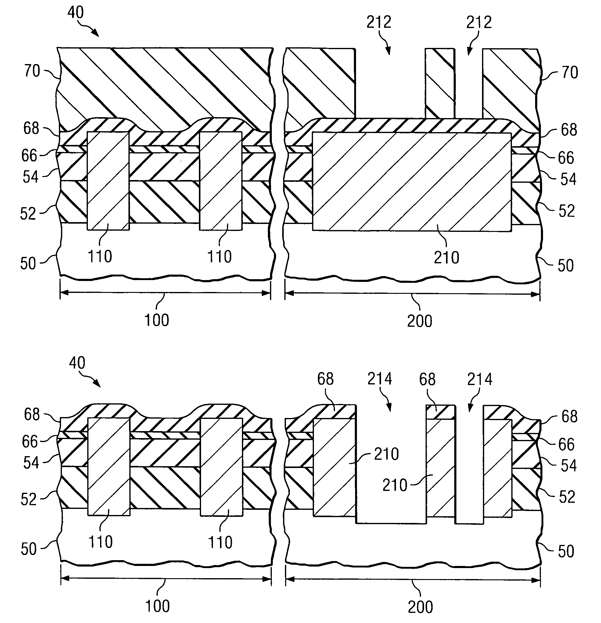
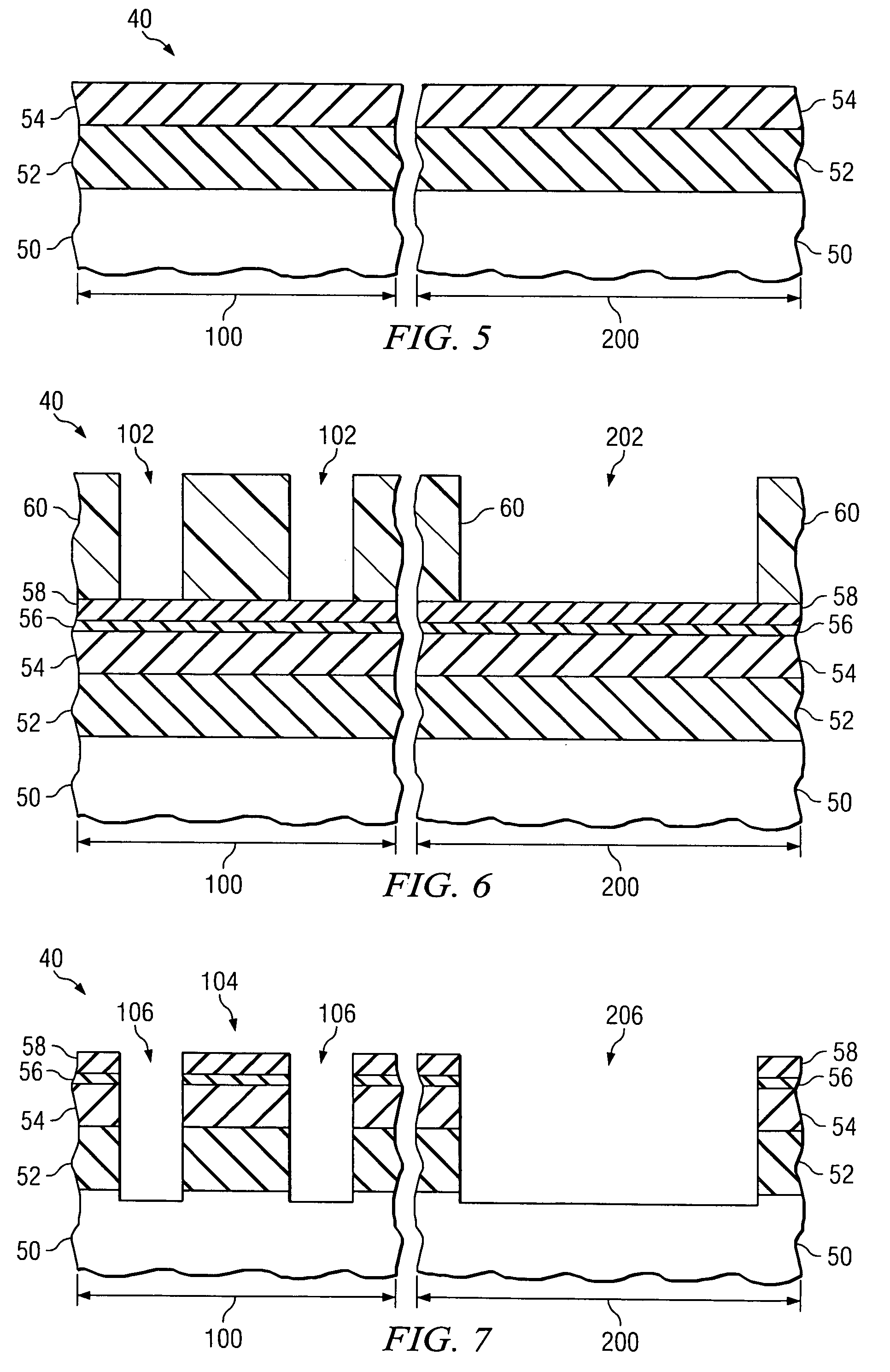
[0021]A novel method of forming a hybrid semiconductor structure having a hybrid crystal orientation and forming high performance MOSFETs on the hybrid semiconductor structure is illustrated in FIGS. 5 through 19. Throughout the various views and illustrative embodiments of the present invention, like reference numbers are used to designate like elements.

[0022]FIG. 5 illustrates a substrate 40 having a well-known SOI structure. The SOI structure includes a buried oxide (BOX) 52 on a semiconductor layer 50. A semiconductor layer 54 is on the BOX 52. In the preferred embodiment...


PUM


Abstract

A method of forming a semiconductor structure having a hybrid crystal orientation and forming MOSFETs having improved performance on the semiconductor structure is provided. The method includes providing a substrate comprising a buried oxide (BOX) on a first semiconductor layer, and a second semiconductor layer on the BOX, wherein the first and second semiconductor layers have a first and a second crystal orientation, respectively, and wherein the substrate comprises a first region and a second region. An isolation structure is formed in the second region extending to the first semiconductor layer. A trench is then formed in the isolation structure, exposing the first semiconductor layer. A semiconductor material is epitaxially grown in the trench. The method further includes forming a MOSFET of a first type on the second semiconductor layer and a MOSFET of an opposite type than the first type on the epitaxially grown semiconductor material.

Description

[0001]This application claims priority to provisional patent application Ser. No. 60 / 693,879, filed Jun. 24, 2005, entitled “High Performance Transistors with Hybrid Crystal Orientations,” which application is hereby incorporated herein by reference.TECHNICAL FIELD[0002]The present invention relates to metal oxide semiconductor field effect transistors (MOSFETs), and more particularly to a method of fabricating a semiconductor structure having a hybrid crystal orientation and fabricating MOSFETs on the semiconductor structure.BACKGROUND[0003]In present semiconductor technology, complementary metal oxide semiconductor (CMOS) devices, such as n-type field effect transistors (FETs) or NFETs, are typically fabricated on semiconductor wafers, such as silicon wafers that have a single crystal orientation, sometimes also referred to as direction. In particular, most of today's semiconductor devices are built on silicon substrates having a (100) crystal orientation.[0004]Electrons are known...

Claims


Application Information

Patent Timeline
Patent Type & Authority Patents(United States)
IPC IPC(8): H01L21/336H01L21/8234
CPCH01L21/823807H01L21/823878H01L29/78H01L29/045H01L21/84
Inventor LIN, CHUNG-TEWU, I-LUSADAKA, MARIAM
Owner TAIWAN SEMICON MFG CO LTD
Why Eureka
Try Eureka