III-nitride compound semiconductor light emitting device

a technology of compound semiconductors and light-emitting devices, which is applied in the direction of solid-state devices, semiconductor lasers, lasers, etc., can solve the problems of increasing the crystalline defect rate, difficult to apply such a technology applied to the gaas-based light-emitting device to the gan-based light-emitting device without hard work, and increasing the external quantum efficiency of the light-emitting device. , to achieve the effect of increasing the external quantum efficiency

Inactive Publication Date: 2009-11-24
EPIVALLEY
View PDF14 Cites 48 Cited by
  • Summary
  • Abstract
  • Description
  • Claims
  • Application Information

AI Technical Summary

Benefits of technology

[0011]In the present invention, by taking notice of an exposed surface of an s n-type Al(x)ln(y)Ga(1-x-y)N layer to which attention has not yet been paid in a GaN based light-emitting device, a roughened surface is formed on the exposed surface. It is therefore possible to increase external quantum efficiency of the light-emitting device.
[0012]Furthermore, a roughened surface can be formed in an etching process for forming an n-type electrode. Therefore, the present invention has an advantageous effect in that external quantum efficiency of a light-emitting device is increased without changing the structure of a GaN based light-emitting device or the need for an additional complex process.

Problems solved by technology

However, a GaN based light-emitting device has lots of limitations in machining an exposed surface unlike a GaAs based light-emitting device.
These limitations may include that it is difficult to machine an n-type layer since a substrate such as sapphire is provided in the n-type layer, growth of a thick p-type GaN layer results in an increase in crystalline defects even though the thick p-type GaN layer is required for machining, etc.
It is therefore difficult to apply such a technology applied to the GaAs based light-emitting device to the GaN based light-emitting device without hard work.
It is, however, difficult to apply an etching technology, which uses polystyrene spheres as a mask, to the GaN based light-emitting device.

Method used


Image

  • III-nitride compound semiconductor light emitting device
  • III-nitride compound semiconductor light emitting device
  • III-nitride compound semiconductor light emitting device

Examples


example 1

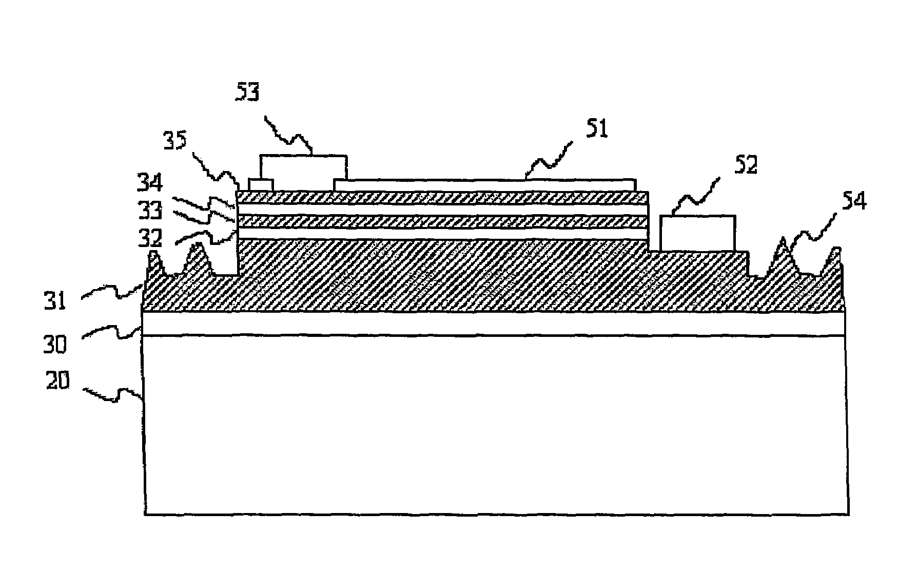
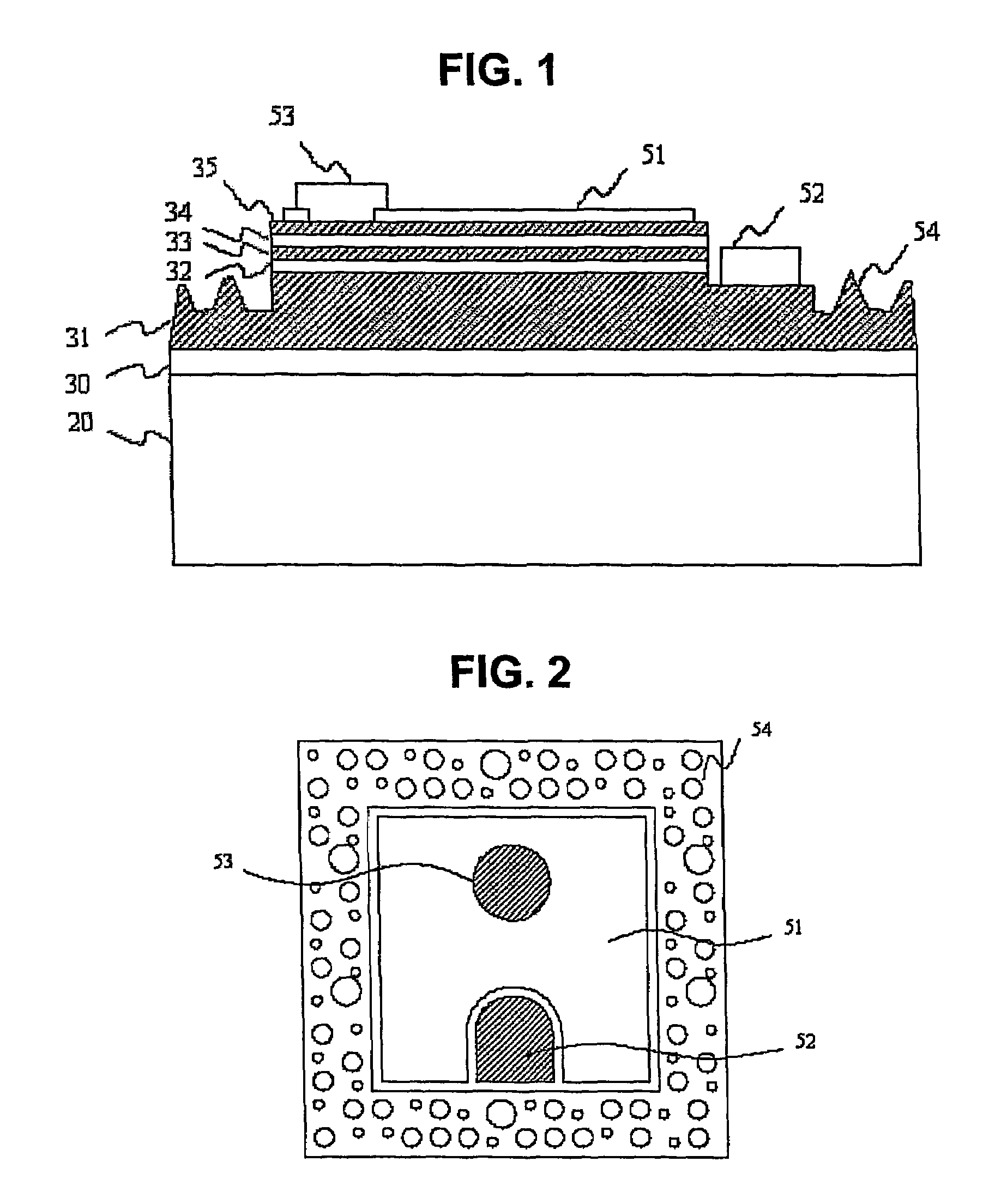
[0027]FIG. 1 is a cross-sectional view of a nitride semiconductor light-emitting device according to a first embodiment of the present invention. FIG. 2 is a plan view of the light-emitting device shown in FIG. 1.

[0028]Referring to FIG. 1, the light-emitting device includes a substrate 20, a buffer layer 30 epitaxially grown on the substrate 20, an n-type Al(x)ln(y)Ga(1-x-y)N layer 31 epitaxially grown on the buffer layer 30, an active layer 33 epitaxially grown on the n-type Al(x)ln(y)Ga(1-x-y)N layer 31, a p-type Al(a)ln(b)Ga(1-a-b)N layer 35 epitaxially grown on the active layer 33, a p-type electrode 51 and a p-type bonding pad 53 that electrically contact with the p-type Al(a)ln(b)Ga(1-a-b)N layer 35, and an n-type electrode 52 that electrically contacts with the n-type Al(x)ln(y)Ga(1-x-y)N layer 31. Also, protrusions 54 are formed on an exposed surface of the n-type Al(x)ln(y)Ga(1-x-y)N layer 31.

[0029]The present invention can be applied to light-emitting devices having a vari...

example 2

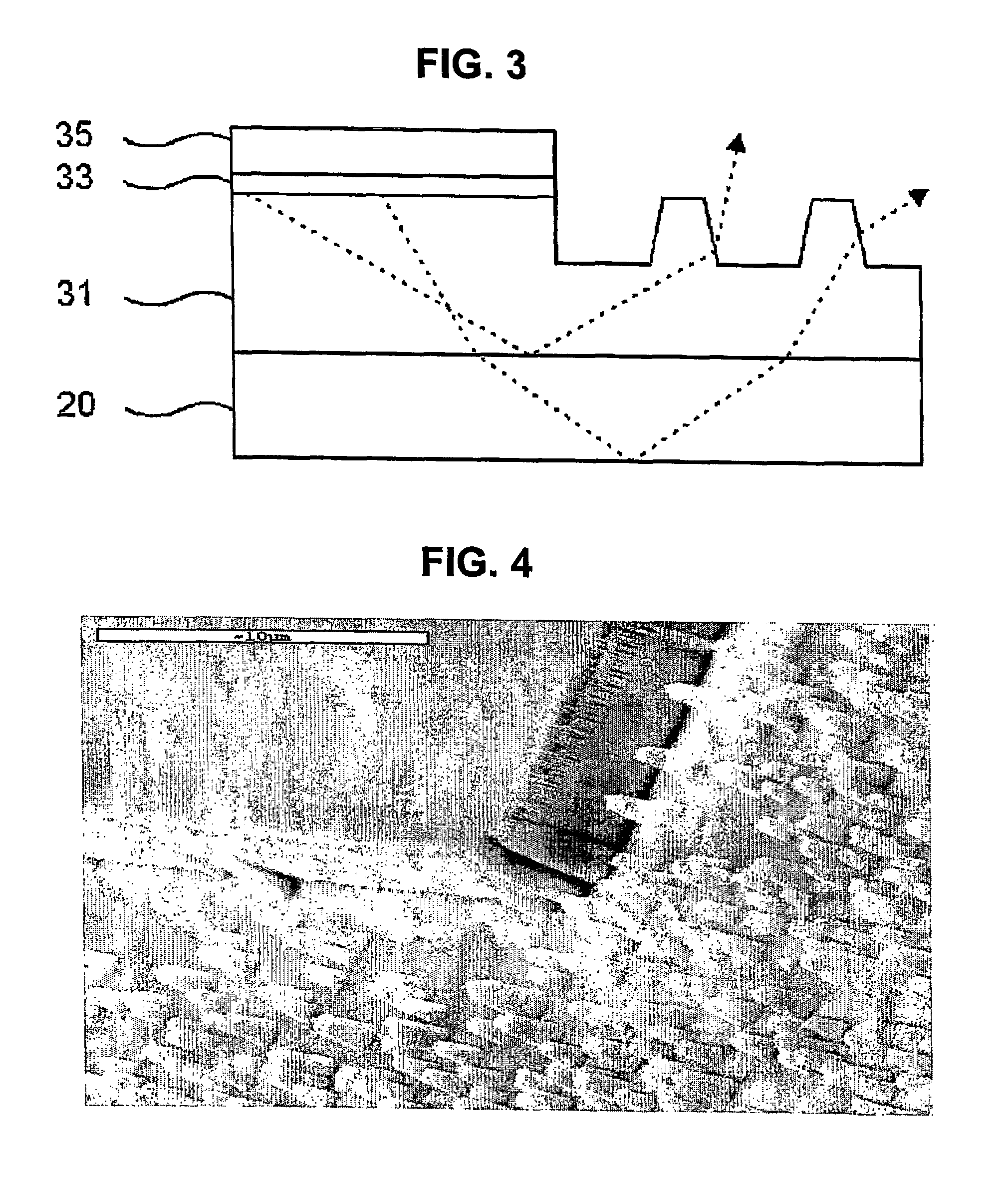
[0040]FIG. 6 is a cross-sectional view showing a nitride semiconductor light-emitting device according to a second embodiment of the present invention. FIG. 7 is a plan view of the light-emitting device shown in FIG. 6. A roughened surface 54B in FIG. 6 is formed by means of photoelectrochemical etching.

[0041]FIG. 8 is a view showing the principle of photoelectrochemical etching that is generated at a portion where the n-type Al(x)ln(y)Ga(1-x-y)N layer 31 and an etch solution 41 contact with each other.

[0042]When an ultraviolet ray 40 is irradiated to the n-type Al(x)ln(y)Ga(1-x-y)N layer 31, electrons and holes are formed on the surface of the n-type Al(x)ln(y)Ga(1-x-y)N layer 31 by means of exitation energy. The electrons (e) formed move into the semiconductor and the holes (h) move to the surface of the semiconductor.

[0043]If the n-type Al(x)ln(y)Ga(1-x-y)N layer 31 is GaN, the holes (h) that moved to the surface of the semiconductor are combined with GaN to separate gallium (Ga)...

example 3

[0049]FIG. 12 is a cross-sectional view of a nitride semiconductor light-emitting device according to a third embodiment of the present invention. FIG. 13 is a plan view of the light-emitting device shown in FIG. 12. Roughened surface 54C in FIG. 12 is formed by surface gratings.

[0050]The shape of the surface grating 54C formed using a mask pattern can be hexagonal, square, triangular or the like and a combination of 2 or 2 or more of them. Each of the surface gratings may have a predetermined size.

[0051]In order to maximize the density of the surface gratings 54C, it is preferred that the shape of the surface grating 54C is hexagonal. Also, it is preferred that the surface area of the surface grating is in the range of 1.5 μm2 to 4 μm2 and the height of the surface grating is in the range of 0.5 μm to 1.5 μm. The portion in which the surface gratings 54C are formed is the edge region other than the region which is the light-emitting portion of the device and the region for contact ...


PUM


Abstract

The present invention relates to a III-nitride semiconductor light-emitting device having high external quantum efficiency, provides a III-nitride compound semiconductor light-emitting device including an active layer generating light by recombination of electrons and holes and containing gallium and nitrogen, an n-type Al(x)ln(y)Ga(1-x-y)N layer epitaxially grown before the active layer is grown, and an n-type electrode electrically contacting with the n-type Al(x)ln(y)Ga(1-x-y)N layer, in which the n-type Al(x)ln(y)Ga(1-x-y)N layer has a surface which is exposed by etching and includes a region for scribing and breaking the device and a region for contact with the n-type electrode, and the surface of the region for scribing and breaking the device is roughened, thereby it is possible to increase external quantum efficiency of the light-emitting device.

Description

TECHNICAL FIELD[0001]The present invention relates to a III-nitride semiconductor light-emitting device, and more particularly, to a III-nitride semiconductor light-emitting device having high external quantum efficiency. The III-nitride compound semiconductor refers to a semiconductor of an Al(x)ln(y)Ga(1-y)N type but may include semiconductors formed using elements of different groups such as SiC, SiN and SiCN or elements themselves.BACKGROUND ART[0002]A variety of attempts have been made to improve external quantum efficiency of a light-emitting device. Among them, methods for roughening an exposed surface of a light-emitting device have been presented.[0003]U.S. Pat. No. 6,504,180 related to a GaAs based light-emitting device discloses a technology wherein at least some of an exposed surface of a light-emitting device is roughened so as to improve external quantum efficiency.[0004]The reason why a desired portion of the exposed surface of the GaAs based light-emitting device can...

Claims


Application Information

Patent Timeline
Patent Type & Authority Patents(United States)
IPC IPC(8): H01L27/15H01L21/311H01S5/00H01L33/22
CPCH01L33/20H01L33/22H01L33/32
Inventor KIM, CHANG-TAEKIM, KEUKJEON, SOO-KUNJANG, PIL-GUKKIM, JONG-WON
Owner EPIVALLEY
Why Eureka
Try Eureka