Structure and manufacturing method of substrate board

a manufacturing method and substrate technology, applied in the direction of resistive material coating, semiconductor/solid-state device details, superimposed coating process, etc., can solve the problems of generating great the variation of heat expansion coefficient between the substrate layer, the heat expansion coefficient between the electrical isolation layer and the heat conduction and electrical isolation layer, etc., to achieve the effect of reducing residual thermal stress within the substrate board, increasing the yield rate of substra

Inactive Publication Date: 2009-12-29
LIN YU HSUEH
View PDF12 Cites 1 Cited by
  • Summary
  • Abstract
  • Description
  • Claims
  • Application Information

AI Technical Summary

Benefits of technology

[0015]The secondary objective of the present invention provides a method for manufacturing a substrate board. Through combining the considerations of forming sequences and the heat expansion characteristics of the materials, the residual thermal stress within the substrate board will be obviously reduced after all manufacturing processes are completed.
[0020]Meanwhile, the actual forming sequences are forming first anodic treatment layer and the second anodic treatment layer, forming the heat conduction and electrical isolation layer, and the DLC layer; moreover, the heat expansion coefficient of the second anodic treatment layer is greater than that of the heat conduction and electrical isolation layer; and the heat expansion coefficient of the heat conduction and electrical isolation layer is greater than that of the (DLC) layer. Therefore, the residual thermal stress within the substrate board can be reduced after all manufacturing processes are completed. Moreover, the second anodic treatment layer is composed of a metallic oxide of a metal, and the heat conduction and electrical isolation layer is made of a metallic nitride of the same metal, so that the heat conduction and electrical isolation layer can be well bonded with the second anodic treatment layer. Basing on above factors, it is not easily to generate the phenomenon of peeling when cutting or trimming the substrate board of the present invention, so as to increase the yield rate of substrate board cutting.

Problems solved by technology

From above description, in the prior arts, it is obvious that the heat conduction performance of the isolation layer is poor, and the variation of heat expansion coefficients between the substrate layer, the electrical isolation layer and the heat conduction and electrical isolation layer, is too great.
First, the great the variation of heat expansion coefficients of the members within the substrate board generate great thermal stress within the substrate board.
Second, the overall heat conduction performance of the substrate layer is poor.

Method used


Image

  • Structure and manufacturing method of substrate board
  • Structure and manufacturing method of substrate board
  • Structure and manufacturing method of substrate board

Examples


first embodiment

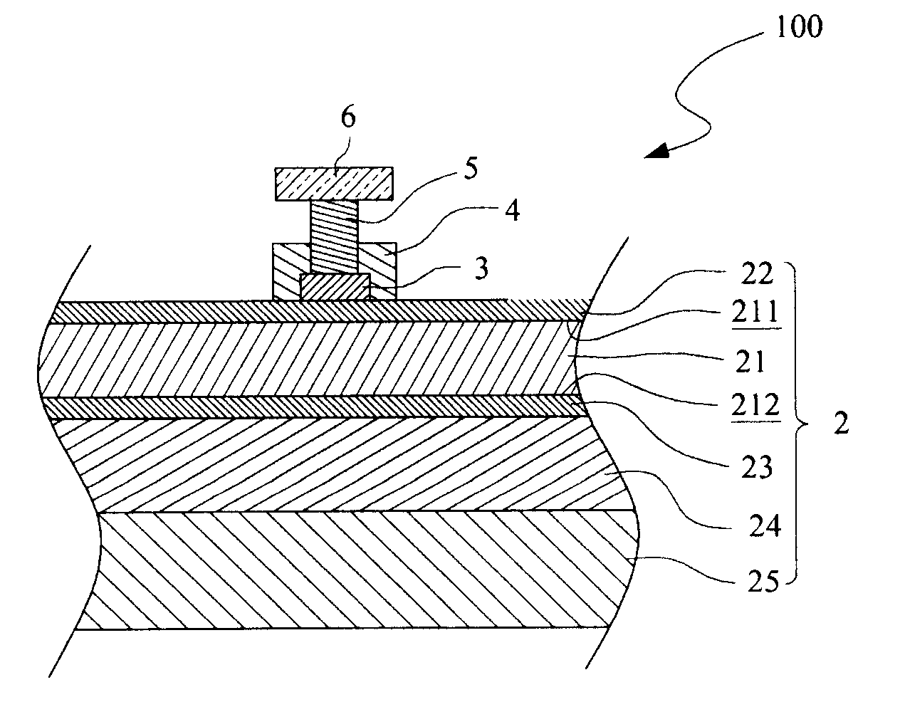
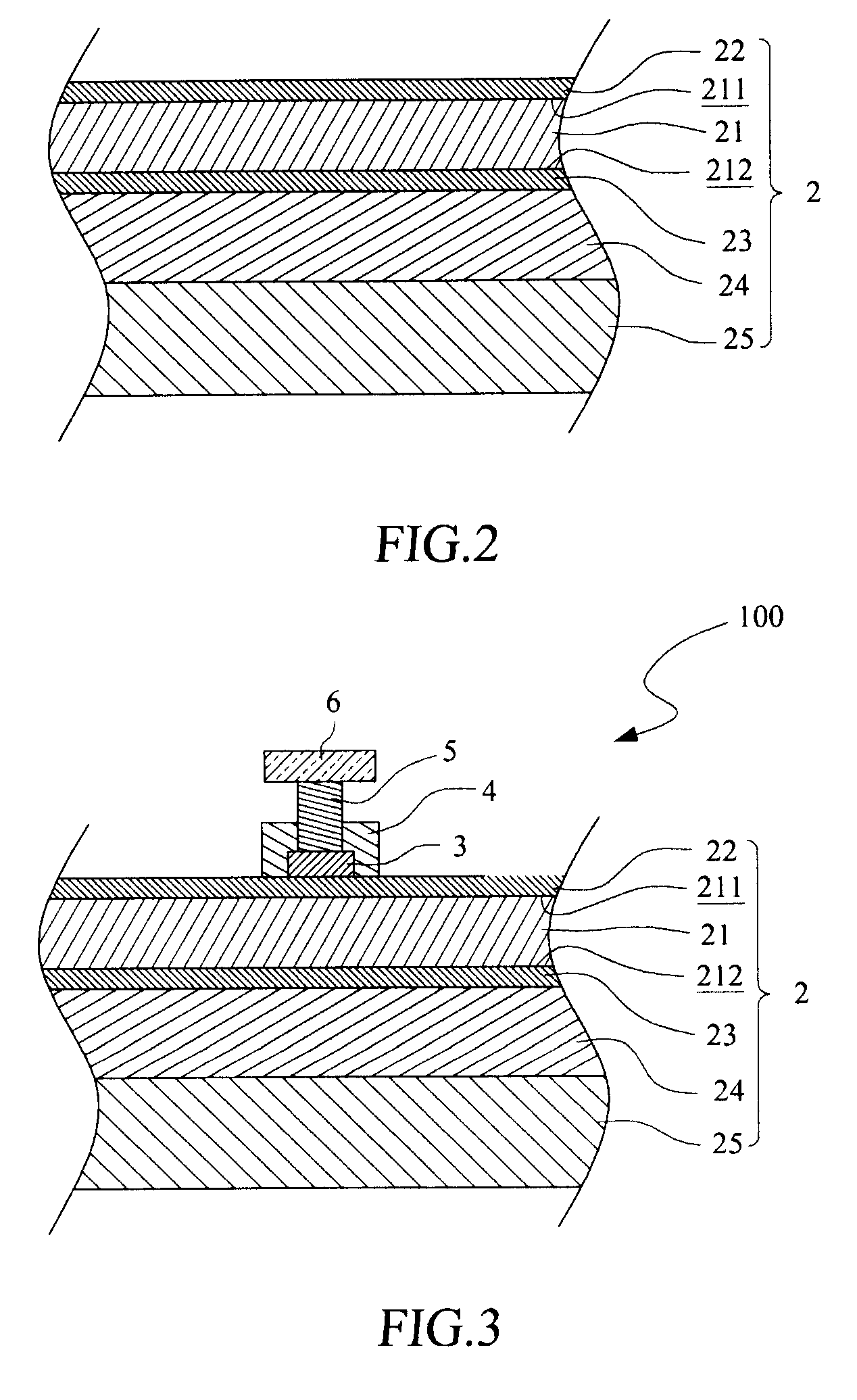
[0033]Preferably, in the first embodiment, the second anodic treatment layer 23 and the heat conduction and electrical isolation layer 24 are respectively composed of the metallic oxide and a metallic nitride of the same metal. For example, the first anodic treatment layer 22 and the second anodic treatment layer 23 can be composed of aluminum oxide (Al2O3); the heat conduction and electrical isolation layer 24 is composed of aluminum nitride (AlN). Obviously, under this condition, the heat conduction and electrical isolation layer 24 can be well bonded with the second anodic treatment layer 23.

[0034]Moreover, when the substrate layer 21 is made of aluminum, the first anodic treatment layer 22 and the second anodic treatment layer 23 are composed of aluminum oxide (Al2O3), the heat conduction and electrical isolation layer 24 is composed of aluminum nitride (AlN), the heat expansion coefficients of the mentioned structural layers are actually measured as follows: the heat expansion ...

second embodiment

[0048]Please refer to FIG. 6, which illustrates a simplified flowchart of manufacturing the substrate board in accordance with the present invention. At the same time, please refer to FIG. 4 and FIG. 5. The method for manufacturing the substrate board 2a comprises the steps as follows. First, provide a substrate layer 21 having the arrangement surface 211 and the heat-dissipating surface 212 (step 110), and execute an anodic treatment to the substrate layer 21, so as to form the first anodic treatment layer 22 and the second anodic treatment layer 23 respectively on the arrangement surface 211 and the heat-dissipating surface 212 (step 120).

[0049]Following up, execute a vacuum-sputter treatment, a plasma vapor deposition (PVD) treatment, a chemical vapor deposition (CVD) treatment, or an ion implantation treatment, so as to form the heat conduction and electrical isolation layer 24 on the second anodic treatment layer 23 (step 130).

[0050]Hereafter, execute a plasma-enhanced chemical...


PUM

PropertyMeasurementUnit
currentaaaaaaaaaa
currentaaaaaaaaaa
wavelengthaaaaaaaaaa

Abstract

A method for manufacturing a substrate board with high efficiency of heat conduction and electrical isolation is disclosed. The method comprises the steps of: providing a substrate layer with an arrangement surface and a heat-dissipating surface; executing an anodic treatment on the arrangement surface and the heat-dissipating surface to respectively form a first anodic treatment layer and a second anodic treatment layer; forming a heat conduction and electrical isolation layer on the second anodic treatment layer; and forming a diamond like carbon (DLC) layer on the heat conduction and electrical isolation layer. The heat expansion coefficient of the substrate layer is greater than that of the second anodic treatment layer, the heat conduction and electrical isolation layer, and the DLC layer in turn.

Description

FIELD OF THE INVENTION[0001]The present invention relates to a technology of manufacturing a substrate board, and more particularly to a technology of manufacturing a substrate board with high efficiency of heat conduction and electrical isolation.BACKGROUND OF THE INVENTION[0002]Among all electronic devices existed in the present, there are many electronic working components assembled therein, such as micro processors, semiconductor chips or light emitting diodes (LEDs), etc., to execute preset assignments. In the practice, it is usually necessary to print a printed circuit on a substrate board, and deposit the electronic components on the printed circuit, so as to manufacture a printed circuit board.[0003]Meanwhile, when the electronic components execute the preset assignments, it is unavoidable to release heat energy. In the most conditions, if heat energy could not be dissipated out of the PCB, it not only influences the normal operations of the electronic components, but also m...

Claims


Application Information

Patent Timeline
Patent Type & Authority Patents(United States)
IPC IPC(8): H05K1/00
CPCH05K1/053H05K7/205H01L23/3732H05K2201/0175H05K2201/0179H01L2924/0002H05K2201/0323H05K2203/0315H01L2924/00
Inventor LIN, YU-HSUEH
Owner LIN YU HSUEH
Why Eureka
Try Eureka