Wired circuit board

a wired circuit board and circuit board technology, applied in the direction of printed circuit aspects, transportation and packaging, chemistry apparatus and processes, etc., can solve the problems of defective adhesion between the lower conductor and the insulating layer, increase the transmission loss of the conductive pattern, etc., to improve the adhesion, reduce the transmission loss, and simple layer structure

Active Publication Date: 2009-12-29
NITTO DENKO CORP
View PDF48 Cites 3 Cited by
  • Summary
  • Abstract
  • Description
  • Claims
  • Application Information

AI Technical Summary

Benefits of technology

[0009]It is therefore an object of the present invention to provide a wired circuit board which can reduce in transmission loss with a simple layer structure and also features excellent long-term reliability by preventing the occurrence of an ion migration phenomenon between a metal foil and an insulating layer to improve the adhesion between the metal foil and the insulating layer and the conductivity of a conductor.
[0012]The wired circuit board according to the present invention can reduce transmission loss. Moreover, since the second metal thin film is formed between the metal foil and the insulating layer, the occurrence of the ion migration phenomenon between the metal foil and the insulating layer is prevented with the simple layer structure. As a result, it is possible to sufficiently improve the adhesion between the metal foil and the insulating layer as well as the conductivity of the conductor to ensure excellent long-term reliability.

Problems solved by technology

In such a suspension board with circuit, a metal supporting board is made of stainless steel, so that a transmission loss is increased in a conductive pattern.
This occasionally causes defective adhesion between the lower conductor and the insulating layer or defective conductivity of the conductors on the recording and playback sides.

Method used


Image

  • Wired circuit board
  • Wired circuit board
  • Wired circuit board

Examples


example 1

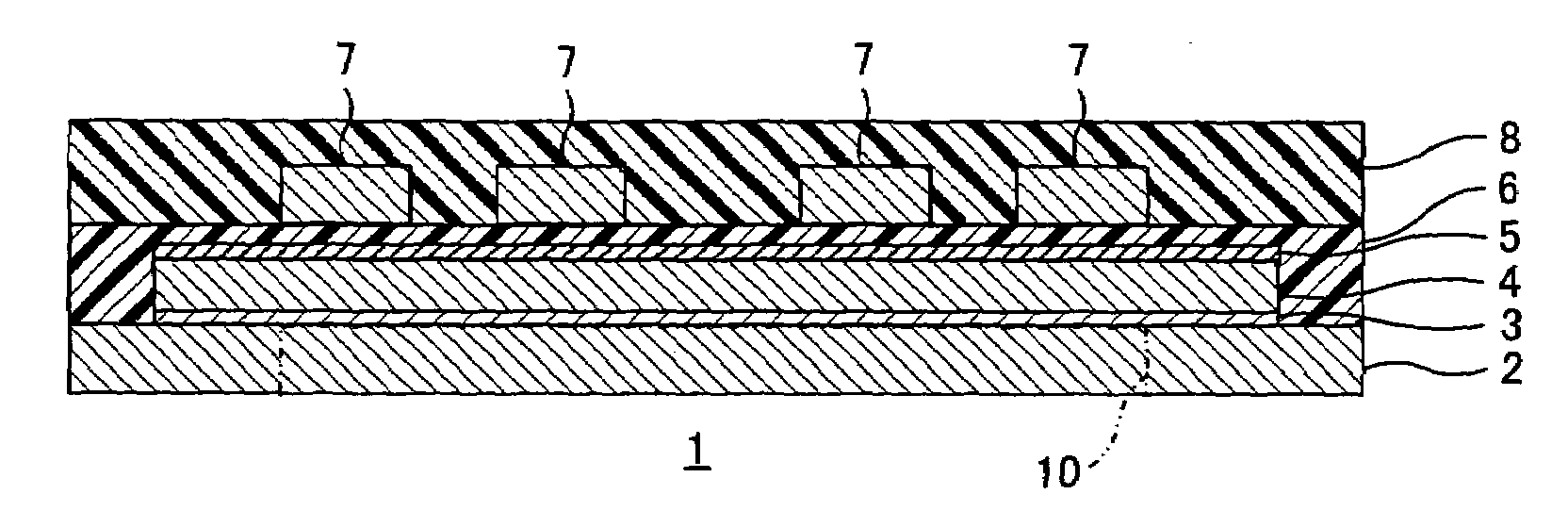
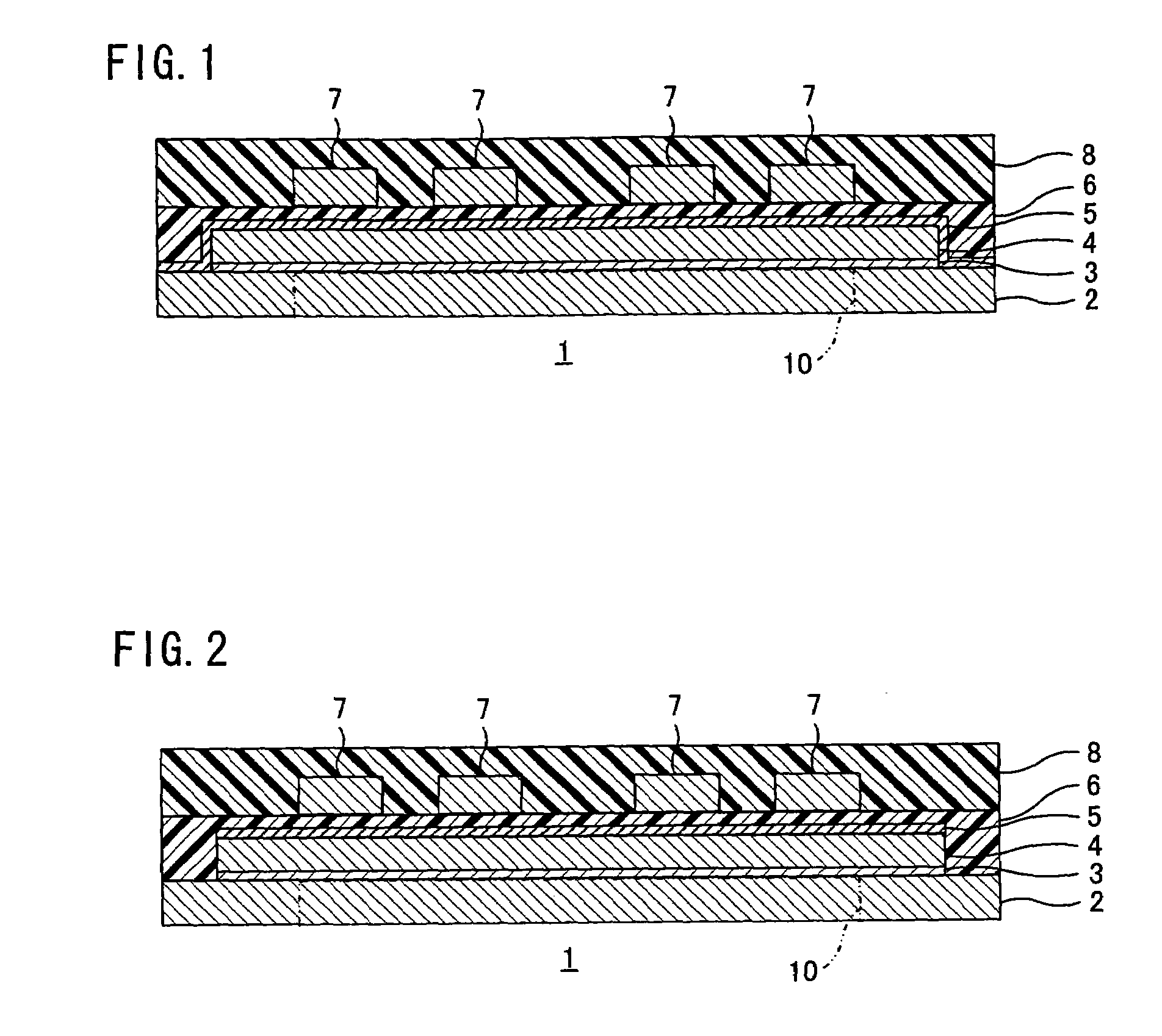
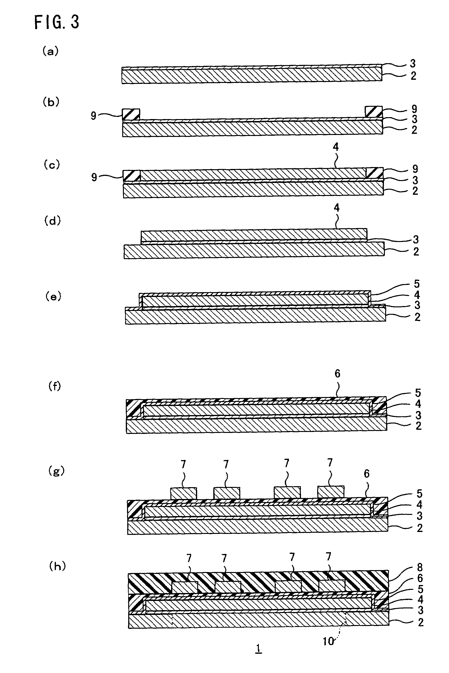
[0055]A chromium thin film with a thickness of 0.03 μm and a copper thin film with a thickness of 0.07 μm were successively formed by sputtering as a first metal thin film on a metal supporting board made of a stainless steel with a thickness of 25 μm (see FIG. 3(a)). A plating resist in a pattern reverse to that of a metal foil was formed using a dry film resist (see FIG. 3(b)). Subsequently, a copper foil with a thickness of 4.0 μm was formed as a metal foil on the entire surface of the portion of the first metal thin film exposed from the plating resist by electrolytic copper plating (see FIG. 3(c)). Then, the plating resist and the portion of the first metal thin film on which the plating resist was formed were removed by chemical etching (see FIG. 3(d)). Thereafter, a nickel thin film with a thickness of 0.1 μm was formed as a second metal thin film over a surface of the metal foil and the metal supporting board by electroless plating (see FIG. 3(e)). Then, a varnish of a photo...

example 2

[0056]A suspension board with circuit was obtained in the same manner as in Example 1 except that a chromium thin film with a thickness of 0.01 μm was formed as the second metal thin film by sputtering.


PUM

PropertyMeasurementUnit
thicknessaaaaaaaaaa
thicknessaaaaaaaaaa
thicknessaaaaaaaaaa

Abstract

A wired circuit board is provided which can reduce transmission loss with a simple layer structure and also features excellent long-term reliability by preventing the occurrence of an ion migration phenomenon between a metal foil and an insulating layer to improve the adhesion between the metal foil and the insulating layer and the conductivity of a conductor. A metal supporting board is prepared and a first metal thin film is formed on the metal supporting board by sputtering or electrolytic plating. A metal foil is formed on the first metal thin film by electrolytic plating. A second metal thin film is formed over the metal foil and the metal supporting board by electroless plating or sputtering. An insulating base layer is formed on the second metal thin film. A conductive pattern is formed as a wired circuit pattern on the insulating base layer. An insulating cover layer is formed on the insulating base layer to cover the conductive pattern.

Description

CROSS REFERENCE TO RELATED APPLICATION[0001]This application claims priority from Japanese Patent Appln. No. 2005-348061, filed Dec. 1, 2005, the contents of which are herein incorporated by reference in their entirety.BACKGROUND OF THE INVENTION[0002]1. Field of the Invention[0003]The present invention relates to a wired circuit board and, more particularly, to a wired circuit board such as a suspension board with circuit.[0004]2. Description of Related Art[0005]There has been conventionally known a suspension board with circuit including a metal supporting board made of stainless steel, an insulating layer made of a resin, and a conductive pattern made of copper, which are formed successively on the metal supporting board.[0006]In such a suspension board with circuit, a metal supporting board is made of stainless steel, so that a transmission loss is increased in a conductive pattern.[0007]To reduce the transmission loss, it has been proposed that a lower conductor made of copper ...

Claims


Application Information

Patent Timeline
Patent Type & Authority Patents(United States)
IPC IPC(8): H01L23/04
CPCH05K1/056H05K3/44H05K3/388Y10T428/24917H05K2201/0338H05K2201/09845H05K2203/0723H05K2201/0317
Inventor ISHII, JUNFUNADA, YASUHITO
Owner NITTO DENKO CORP
Why Eureka
Try Eureka