

Field effect transistors (FETS) with inverted source/drain metallic contacts, and method of fabricating same
a field effect transistor and metal contact technology, applied in the field of improved field effect transistors, can solve the problems of continuous size reduction of semiconductor devices, achieve the effect of reducing the number of source/drain metal contacts, reducing the total contact layout area, and reducing the effect of effective contact area
- Summary
- Abstract
- Description
- Claims
- Application Information
AI Technical Summary
Benefits of technology
Problems solved by technology
Method used
Image

Examples
Embodiment Construction
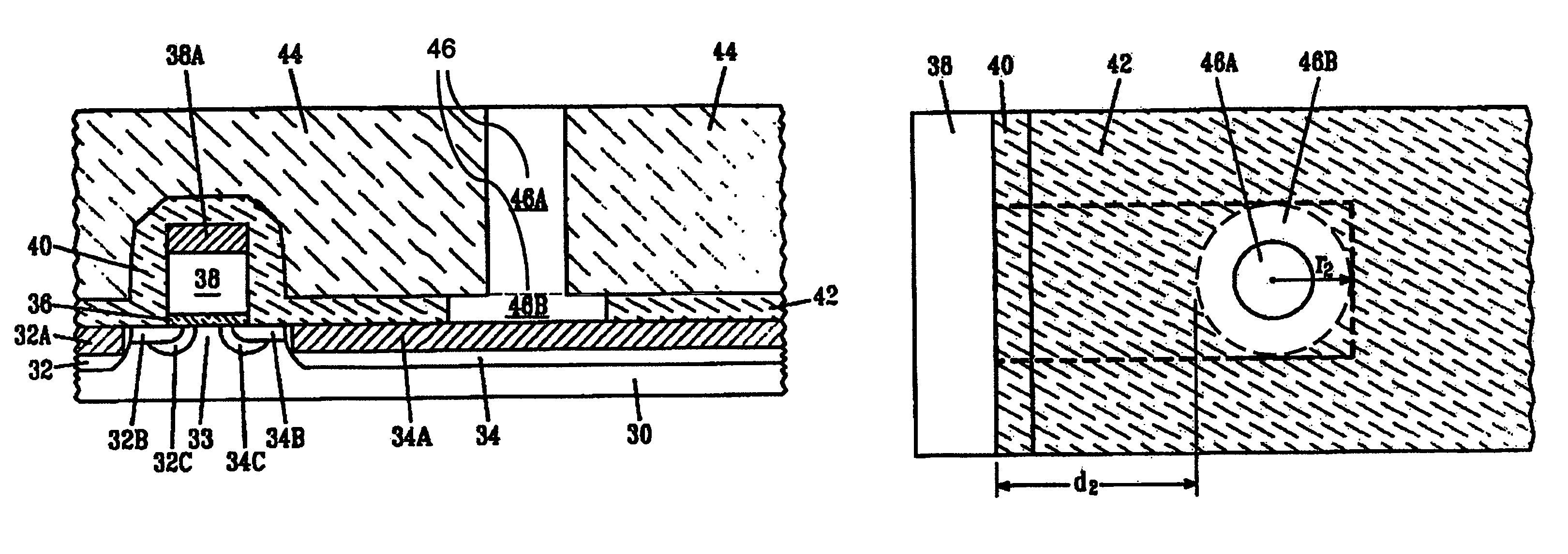
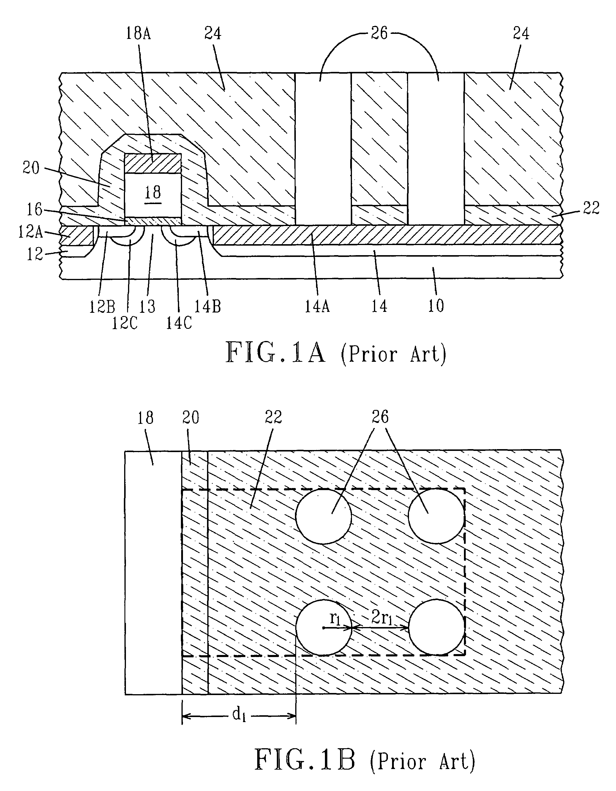
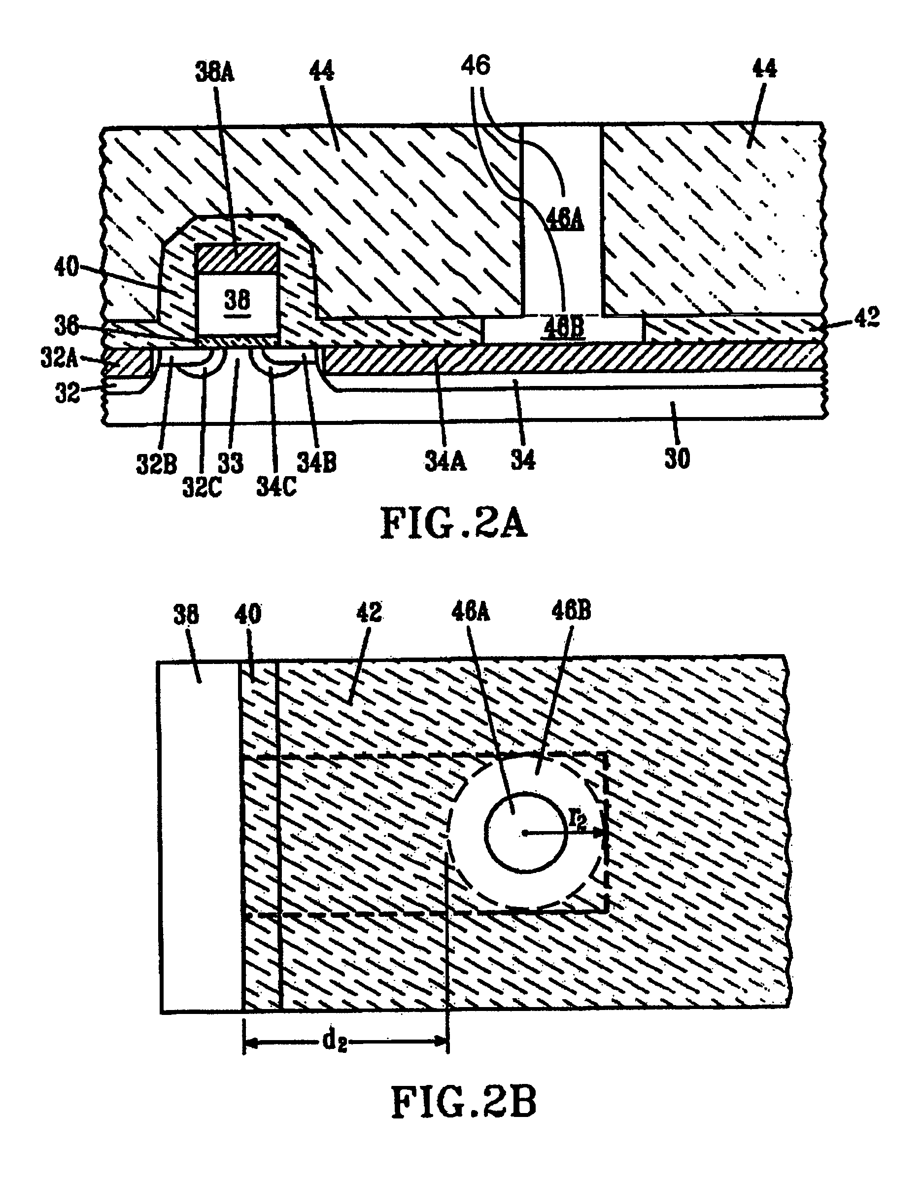
[0026]In the following description, numerous specific details are set forth, such as particular structures, components, materials, dimensions, processing steps and techniques, in order to provide a thorough understanding of the present invention. However, it will be appreciated by one of ordinary skill in the art that the invention may be practiced without these specific details. In other instances, well-known structures or processing steps have not been described in detail in order to avoid obscuring the invention.
[0027]It will be understood that when an element as a layer, region or substrate is referred to as being “on” another element, it can be directly on the other element or intervening elements may also be present. In contrast, when an element is referred to as being “directly on” another element, there are no intervening elements present. It will also be understood that when an element is referred to as being “connected” or “coupled” to another element, it can be directly c...
PUM
| Property | Measurement | Unit |
|---|---|---|
| cross-sectional diameter | aaaaa | aaaaa |
| distance | aaaaa | aaaaa |
| cross-sectional diameter | aaaaa | aaaaa |
Abstract
Description
Claims
Application Information