Piezoelectrics oscillator, sensor, and multi-sensor

a multi-sensor, piezoelectric technology, applied in the direction of vibration measurement in solids, generators/motors, instruments, etc., can solve the problems of reducing the efficiency of the space, increasing the number of manufacturing steps, and difficult miniaturization, so as to improve the space efficiency and compact piezoelectric

Active Publication Date: 2010-02-09
SEIKO EPSON CORP
View PDF21 Cites 16 Cited by
  • Summary
  • Abstract
  • Description
  • Claims
  • Application Information

AI Technical Summary

Benefits of technology

[0012]An advantage of the present invention is to provide a piezoelectric oscillator, a sensor, and a multi-sensor that have excellent productivity. Another advantage is to provide a compact piezoelectric oscillator, a compact sensor, and a compact multi-sensor.
[0013]A piezoelectric oscillator according to a first aspect of the invention includes: a piezoelectric substrate having at least a vibrating part and a base part; an excitation electrode formed on the vibrating part; and an oscillation circuit formed on the base part. In the piezoelectric oscillator, the oscillation circuit includes a thin film transistor made of one of polysilicon and monocrystalline silicon and is coupled to the excitation electrode.
[0014]Since the piezoelectric oscillator is provided with the excitation electrode and the oscillation circuit on its piezoelectric substrate as above, the piezoelectric substrate and the oscillation circuit are unified, improving the space efficiency. Thus the piezoelectric oscillator can be miniaturized. In addition, in the piezoelectric oscillator, the piezoelectric substrate and the oscillation circuit are unified and thus the number of manufacturing steps is reduced due to the reduced number of components, improving the productivity.
[0015]Further, because of the unification of the piezoelectric substrate and the oscillation circuit, the excitation electrode and the oscillation circuit are coupled at a short distance. Therefore, electromagnetic interference between the connecting patterns is suppressed. Thus the performance of the piezoelectric oscillator can be enhanced.
[0016]In the piezoelectric oscillator of the first aspect, the piezoelectric substrate may be an AT cut quartz substrate.
[0017]Since the piezoelectric substrate is the AT cut quartz substrate, the piezoelectric oscillator has small frequency change with respect to the temperature change of the surroundings and the frequency can be increased by thinning the thickness of the substrate. Thus a high frequency oscillator having a desirable temperature property can be easily realized.

Problems solved by technology

That is, in this structure, the package needs a space for storing the piezoelectric substrate and a space for storing the electronic component separately therein, making the further miniaturization difficult.
Further, since the electronic component is a discrete component and is provided in a great number, the number of manufacturing steps increases to degrade the productivity.
In addition, since the discrete component is commonly thick, it is hard to thin the crystal oscillator.
Furthermore, a circuit pattern for wiring a plurality of discrete components becomes complex so as to generate electromagnetic coupling between circuit patterns, deteriorating the performance of the oscillator disadvantageously.
The mass measuring chip (hereinafter, referred to as a sensor) disclosed in the second example has such structure that the piezoelectric resonator element and the IC chip constituting the oscillation circuit are bonded separately to the flat plate, so that the structure hardly satisfies suitable manufacturing efficiency.
In addition, the sensor mounts the piezoelectric resonator element on the flat plate, being hard to be thinned.

Method used


Image

  • Piezoelectrics oscillator, sensor, and multi-sensor
  • Piezoelectrics oscillator, sensor, and multi-sensor
  • Piezoelectrics oscillator, sensor, and multi-sensor

Examples


first embodiment

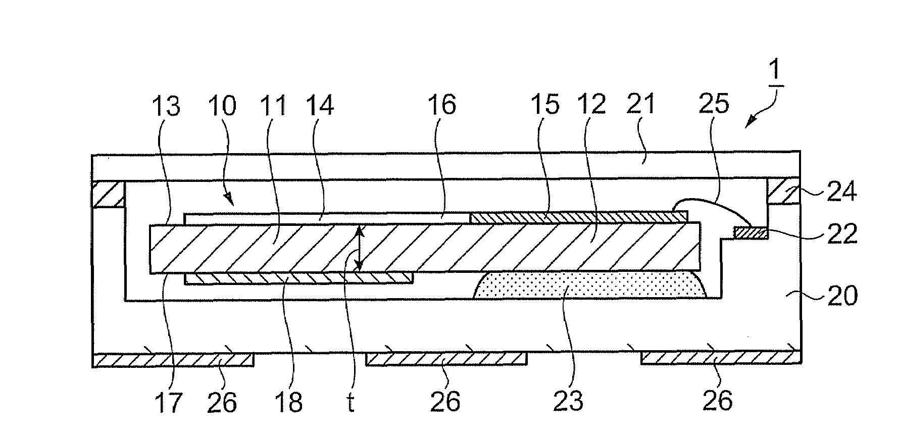
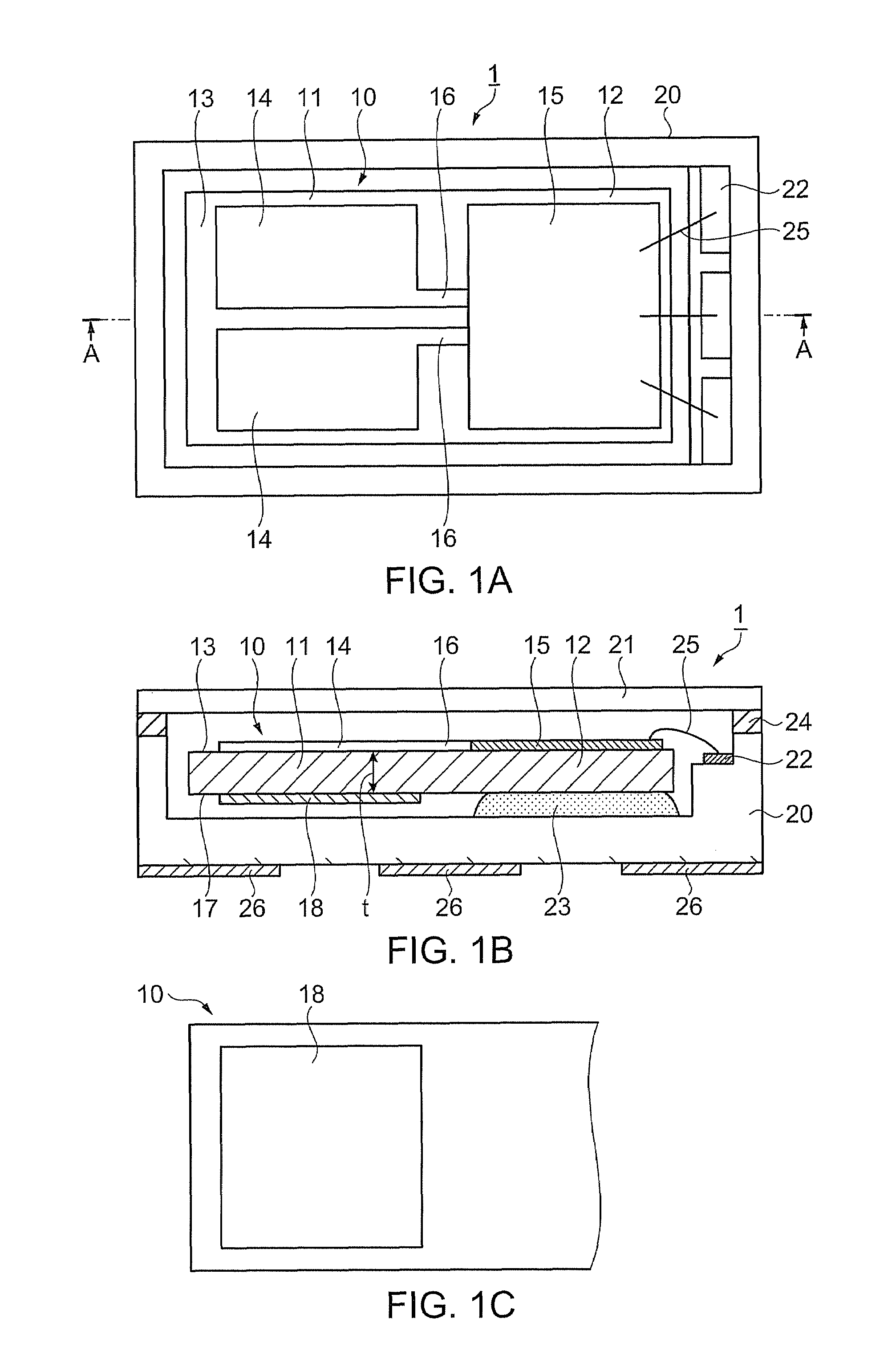
[0054]FIGS. 1A to 1C are schematic views showing a structure of a crystal oscillator as a piezoelectric oscillator according to a first embodiment of the invention. FIG. 1A is a perspective plane view, FIG. 1B is a sectional view taken along the line A-A of FIG. 1A, and FIG. 1C is a back view of the main part of FIG. 1A.

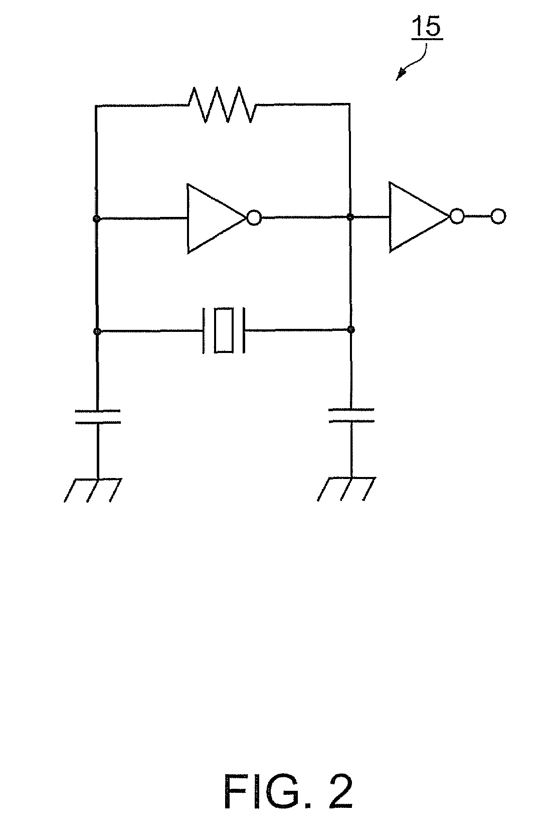
[0055]FIG. 2 is a schematic view showing a structure of an oscillation circuit of the crystal oscillator.

[0056]In each figure including FIGS. 1A to 1C, dimensional ratio of respective elements differs so as to clearly show the structure.

[0057]

[0058]As shown in FIGS. 1A to 1C, this crystal oscillator 1 includes a quartz substrate 10 as a piezoelectric substrate, a package 20, a lid 21, and the like.

[0059]The quartz substrate 10 is fixed to the package 20 at a base part 12 side thereof by an adhesive 23 within the package 20. The adhesive 23 is applied to the base part 12 side so as not to disturb vibration (oscillation) of a vibrating part 11.

[0060]The lid 21 is bonde...

second embodiment

[0093]FIGS. 3A to 3C are schematic views showing a structure of a chemical sensor that detects an organic solvent molecule in vapor phase and employs a piezoelectric oscillator according to a second embodiment of the invention. FIG. 3A is a front plane view, FIG. 3B is a sectional view taken along the line B-B of FIG. 3A, and FIG. 3C is a back plane view. In FIG. 3A, some elements are omitted so as to show the drawing comprehensible.

[0094]

[0095]As shown in FIGS. 3A to 3C, this chemical sensor 101 includes a quartz substrate 110 as a piezoelectric substrate, a sealing plate 121 as a lid member, an adhesive 122, and the like.

[0096]The chemical sensor 101 of the second embodiment includes a sensitive film 30 on its common electrode 118 provided on the quartz substrate 110 that has a similar structure to the quartz substrate 10 of the crystal oscillator 1 of the first embodiment. The quartz substrate 110 is manufactured by the semiconductor process in a similar manner to the quartz subs...

third embodiment

[0141]FIGS. 4A to 4C are schematic views showing a structure of a multi-sensor employing a piezoelectric oscillator according to a third embodiment of the invention. The multi-sensor includes a plurality of chemical sensors that detect a molecule in vapor phase and are provided on a quarts substrate as a large format piezoelectric substrate.

[0142]FIG. 4A is a front plane view, FIG. 4B is a sectional view taken along the line C-C of FIG. 4A, and FIG. 4C is a back plane view. In FIG. 4A, some elements are omitted so as to show the drawing comprehensible.

[0143]

[0144]As shown in FIGS. 4A to 4C, this multi-sensor 201 of the third embodiment includes two chemical sensors 101 of the second embodiment provided to one quartz substrate 210. Therefore, differences from the second embodiment will be primarily described below.

[0145]The multi-sensor 201 includes the quartz substrate 210 that is an AT cut quartz substrate. The quartz substrate 210 is provided with two recesses 211a, 211b (inverted...


PUM


Abstract

A piezoelectric oscillator includes: a piezoelectric substrate having at least a vibrating part and a base part; an excitation electrode formed on the vibrating part; and an oscillation circuit formed on the base part. In the piezoelectric oscillator, the oscillation circuit includes a thin film transistor made of one of polysilicon and monocrystalline silicon and is coupled to the excitation electrode.

Description

[0001]The entire disclosure of Japanese Patent Application No. 2007-074126, filed Mar. 22, 2007 is expressly incorporated by reference herein.BACKGROUND[0002]1. Technical Field[0003]The present invention relates to a piezoelectric oscillator, and a sensor and a multi-sensor that employ a piezoelectric oscillator.[0004]2. Related Art[0005]In recent years, as accompanied with miniaturization of electronic devices, miniaturization of piezoelectric oscillators such as a crystal oscillator mounted on electronic devices has been increasingly required.[0006]In order to meet such requirement, JP-A-10-75120, as a first example, discloses a crystal oscillator that stores a crystal vibrator and an electronic component constituting an oscillation circuit in one container.[0007]In addition, miniaturization of sensors employing a piezoelectric oscillator has been required. For the miniaturization thereof, JP-A-2004-264255, as a second example, discloses a mass measuring chip in which a piezoelect...

Claims


Application Information

Patent Timeline
Patent Type & Authority Patents(United States)
IPC IPC(8): H01L41/08
CPCG01N29/022G01N29/223H03H9/0542H03H9/1007H03H9/1021H03H9/132G01N2291/014G01N2291/021H03H2003/0428
Inventor KONDO, TAKAYUKI
Owner SEIKO EPSON CORP
Why Eureka
Try Eureka