Method and system for implementing metal fill

a metal filling and metal technology, applied in the field of integrated circuit design and manufacture, can solve the problems of affecting the production process of cmp, affecting the performance of cmp, etc., and achieves the effect of reducing local step height, reducing yield and impact circuit performance, and reducing layout pattern dependent dielectric thickness variation

Active Publication Date: 2010-02-09
CADENCE DESIGN SYST INC
View PDF14 Cites 19 Cited by
  • Summary
  • Abstract
  • Description
  • Claims
  • Application Information

AI Technical Summary

Benefits of technology

[0002]In recent years, in integrated circuit (IC) manufacturing, chemical-mechanical polishing (CMP) has emerged as an important technique for planarizing dielectrics because of its effectiveness in reducing local step height and achieving a measure of global planarization not normally possible with spin-on and resist etch back techniques. However, CMP processes have been hampered by layout pattern dependent variation in the inter-level dielectric (ILD) thickness which can reduce yield and impact circuit performance.
[0003]Metal-fill patterning is a common approach for reducing layout pattern dependent dielectric thick...

Problems solved by technology

However, CMP processes have been hampered by layout pattern dependent variation in the inter-level dielectric (ILD) thickness which can reduce yield and impact circuit performance.
However, too much metal may cause dishing to occur.
However, the ECO process is much more complicated for designs that include dummy metal fill geometries to control the effects of on-chip variation (OCV), such as IC designs for processes that use CMP.
One significant problem with this approach is that the process of first removing the original dummy...

Method used


Image

  • Method and system for implementing metal fill
  • Method and system for implementing metal fill
  • Method and system for implementing metal fill

Examples


Embodiment Construction

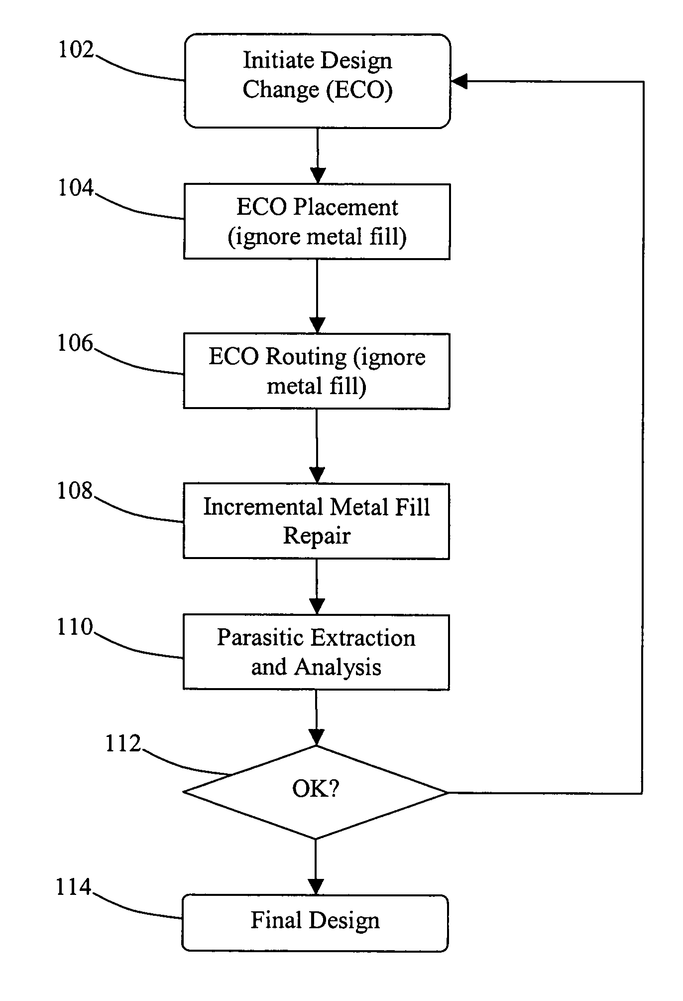
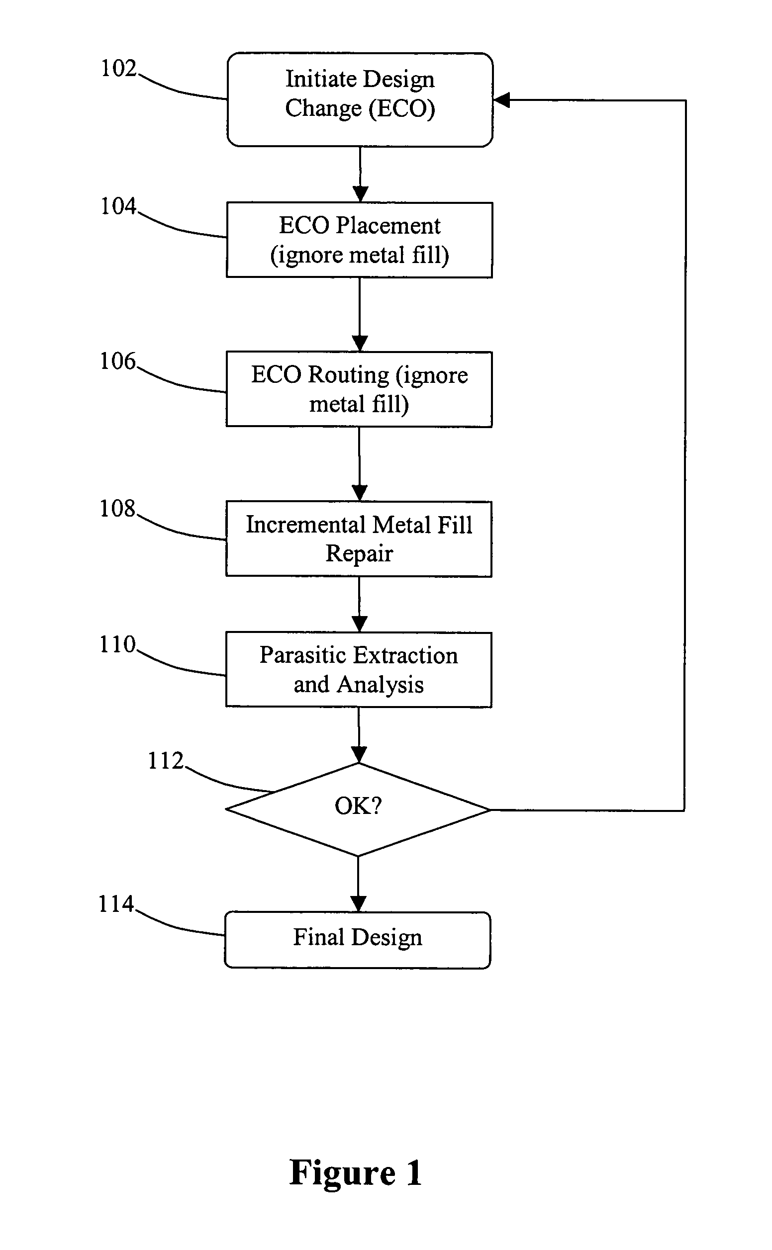
[0020]Disclosed is an improved method and system for implementing metal fill for an integrated circuit design. In some embodiments, when an engineering change order is implemented, the existing dummy metal fill geometries are initially ignored when modifying the layout, even if this results in shorts and / or other DRC violations. Once the ECO changes have been implemented, those violations caused by interaction between the changes and the metal fill are repaired afterwards.

[0021]FIG. 1 is a high-level flow of a process to implement metal fill according to some embodiments of the invention. The disclosed process involves modifying the standard behavior of one or more electronic design automation (EDA) tools in the ECO flow.

[0022]At 102, the ECO change process is initiated, e.g., to update ECO connectivity. Any suitable or conventional approach can be taken to initiate the ECO process. As noted above, the ECO changes may be desired or initiated, for example, to correct an existing prob...


PUM


Abstract

Disclosed is an improved method and system for implementing metal fill for an integrated circuit design. When an engineering change order is implemented, the existing dummy metal fill geometries are initially ignored when modifying the layout, even if this results in shorts and/or other DRC violations. Once the ECO changes have been implemented, those violations caused by interaction between the changes and the metal fill are repaired afterwards.

Description

BACKGROUND AND SUMMARY[0001]The invention relates to the design and manufacture of integrated circuits, and more particularly, to techniques, systems, and methods for implementing metal-fill on an integrated circuit.[0002]In recent years, in integrated circuit (IC) manufacturing, chemical-mechanical polishing (CMP) has emerged as an important technique for planarizing dielectrics because of its effectiveness in reducing local step height and achieving a measure of global planarization not normally possible with spin-on and resist etch back techniques. However, CMP processes have been hampered by layout pattern dependent variation in the inter-level dielectric (ILD) thickness which can reduce yield and impact circuit performance.[0003]Metal-fill patterning is a common approach for reducing layout pattern dependent dielectric thickness variation. Metal-fill patterning is the process of filling large open areas on each metal layer with a metal pattern to compensate for pattern-driven v...

Claims


Application Information

Patent Timeline
IPC IPC(8): G06F17/50G06F9/45
CPCG06F17/5068Y02P90/265G06F2217/12G06F2119/18G06F30/39Y02P90/02
Inventor NOICE, DAVID C.KAO, WILLIAMSEO, INHWANDONG, XIAOPENGNUNN, GARY W.
Owner CADENCE DESIGN SYST INC
Why Eureka
Try Eureka