Trench MOSFET with sidewall spacer gates

a technology of sidewall spacers and mosfets, which is applied in the direction of semiconductor devices, semiconductor/solid-state device details, electrical apparatus, etc., can solve the problems of difficult to reduce this overlap/gate-drain charge, trench defects, and often complicated process sequences for gate insulation layers with varying thicknesses. , to achieve the effect of reducing the gate charge (qgd), reducing the size, and reducing the gate charge (qg) of the electrod

Active Publication Date: 2010-03-02
INFINEON TECH AMERICAS CORP
View PDF8 Cites 4 Cited by
  • Summary
  • Abstract
  • Description
  • Claims
  • Application Information

AI Technical Summary

Benefits of technology

[0016]A gate insulation body is disposed within the void of each gate trench and covers the outer surfaces of the spacer gate therein. According to an embodiment of the invention, a silicide layer may also cover the full outer surfaces of the spacer gate to substantially reduce the gate resistance (Rg) of the gate.
[0018]Advantageously, the spacer gates of the present invention have several benefits as compared to semiconductor devices of the prior art. For example, because the spacer gates do not extend along a portion of the bottom surfaces of the gate trenches, there is minimal overlap between the drain epi region and the gate electrodes, thereby reducing the gate-drain charge (Qgd) of the device. In addition, because the spacer gates are formed as a thin layer of polysilicon rather than as a thick polysilicon gate mass, the gates have a reduced size thereby reducing the gate charge (Qg) of the electrodes and thereby improving the efficiency of the device. In addition, the thin layer of polysilicon is easier to deposit as compared to the thick polysilicon gate mass, resulting in fewer problems with voids forming in the polysilicon that can trap charge and cause instabilities in the threshold voltage (Vt) and drain-to-source leakage current (Idss) of the device.
[0019]According to another embodiment of the invention, the spacer gates of the present invention may allow the trench width and / or trench depth of the gate trenches to be increased (as compared to prior art semiconductor devices) without sacrificing device performance. Specifically, because the spacer gates are formed of a thin layer of polysilicon along the gate trench sidewalls, the width and / or depth of the gate trenches may be increased without increasing the size of the gate electrodes and thereby without increasing the gate charge and gate-drain charge of the device.
[0020]According to another embodiment of the invention, a power semiconductor device is as described above but further includes a trench tip implant formed in the drain epi region at the bottom of each gate trench. The trench tip implants have the same conductivity as the drain epi region and serve to control the gate to drain overlap independent of the depth of the gate trenches, thereby allowing the gate trenches to be made shallower with respect to the depth of the channel region. Notably, the trench tip implant at the bottom of each trench may be formed by using the spacer gate therein as a mask. As a result, the trench tip implant is aligned to the spacer gate. According to a further embodiment of the invention, the device may also include a deep body implant formed in the channel region along the junction with the drain epi region. The deep body implant has the same conductivity as the channel region and serves to reduce the intensity of the electric fields at the bottom of the gate trenches and along the junction of the channel and drain epi regions, thereby improving the breakdown voltage of the device.

Problems solved by technology

Nonetheless, it can be difficult to reduce this overlap / gate-drain charge.
However, the cleaning of thin gate trenches during device fabrication can be difficult, leading to trench defects.
Unfortunately, the fabrication of a gate insulation layer 24 with varying thicknesses is often a complicated process sequence.
However, as also described above, the use of thin trenches can lead to trench defects.
In general, it can be difficult to control the polysilicon recess depth to obtain this overlap when etching back a thick polysilicon gate mass.
Another problem with thick polysilicon gates 26 is that voids may form in the polysilicon as the polysilicon is deposited into the trenches 12.
Such voids can trap charge that cause instabilities in the threshold voltage (Vt) and drain-to-source leakage current (Idss) of the device.
However, it can be difficult to control the trench etch depth to obtain sufficient overlap while not over etching the trenches.
Again, over etching the trenches results in larger gate electrodes and thereby increased gate-drain charge and increased gate charge.

Method used


Image

  • Trench MOSFET with sidewall spacer gates
  • Trench MOSFET with sidewall spacer gates
  • Trench MOSFET with sidewall spacer gates

Examples


Embodiment Construction

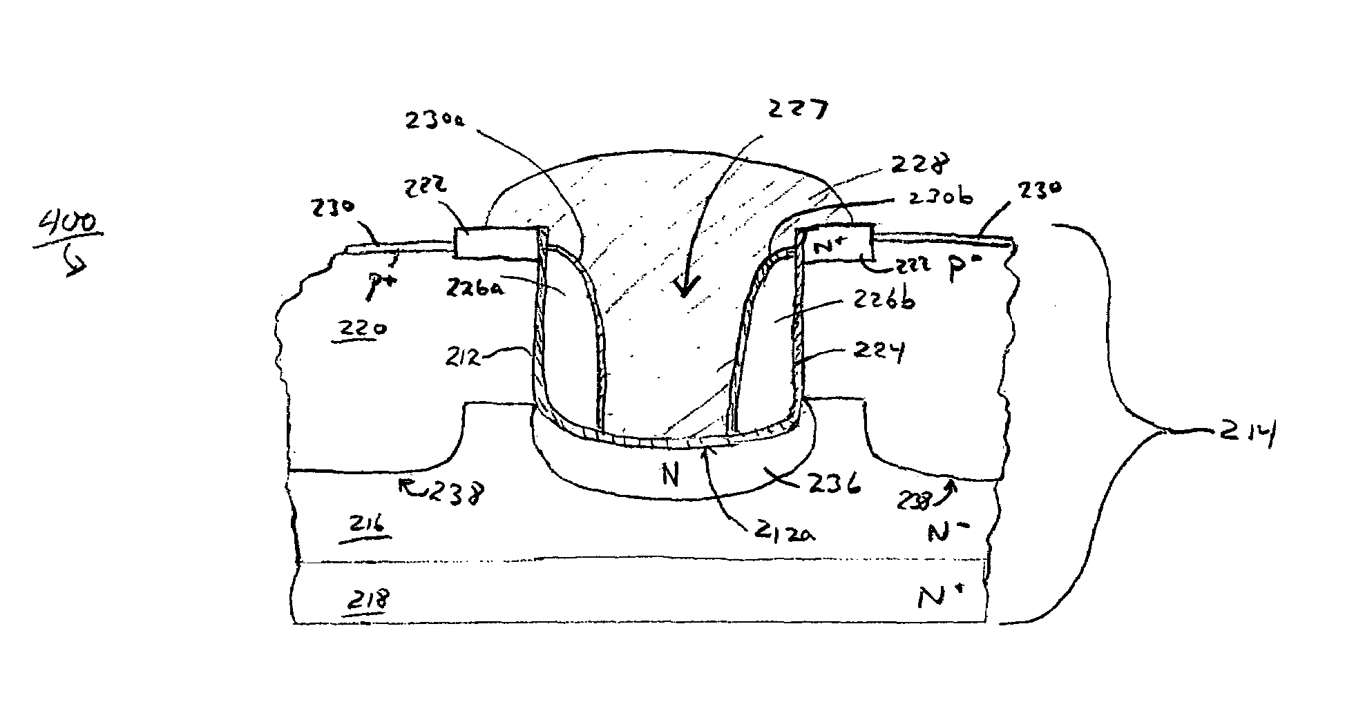
[0026]Referring to FIG. 2 there is shown a cross-sectional side view of a portion of an active region of a power semiconductor device 200, such as a MOSFET, according to an embodiment of the invention. Device 200 includes a semiconductor body 214 that may be made of silicon or silicon carbide, for example. The exact configuration of body 214 is not specific to the invention. As an example, body 214 may include a drain epi region 216 of one conductivity (e.g. N-type) formed over a silicon substrate 218 of the same conductivity, but of higher concentration of impurities. A channel / body region 220 may be formed in drain epi region 216 that extends from the top surface of the semiconductor body to a first depth. Channel region 220 has a conductivity opposite to that of drain epi region 216 (e.g. P-type). Formed within channel region 220 are source regions 222, which have the same conductivity (e.g. N-type) as drain epi region 216. Device 200 may further include high conductivity contact...


PUM


Abstract

A semiconductor power device includes a semiconductor body with a plurality of gate trenches formed therein. Disposed within each gate trench is a spacer gate that extends along at least a portion of the sidewalls of the gate trench but not along at least a portion of the bottom surface of the trench. The spacer gate of each gate trench may also include a layer of silicide along outer surfaces thereof. The semiconductor body may include a channel region and each gate trench may extend through the channel region and into the semiconductor body. Formed at the bottom of each gate trench within the semiconductor body may be a tip implant of the same conductivity as the semiconductor body. In addition, a deep body implant of the same conductivity as the channel region may be formed at the base of the channel region.

Description

RELATED APPLICATION[0001]This application is based on and claims benefit of U.S. Provisional Application No. 60 / 668,724, filed on Apr. 5, 2005, entitled “TRENCH MOSFET WITH POLYSILICON SIDEWALLS IN TRENCH AND SILICIDE SURFACES ON SIDEWALLS,” by Timothy D. Henson to which a claim of priority is hereby made and the disclosure of which is incorporated by reference.BACKGROUND OF THE INVENTION[0002]1. Field of the Invention[0003]The present invention relates generally to semiconductor devices, and more specifically, to trench type power semiconductor devices with sidewall spacer gates and a method for fabricating the same.[0004]2. Description of the Prior Art[0005]Trench type power semiconductor devices such as power MOSFETs are well known. For example, referring to FIG. 1 there is shown a portion of a power MOSFET 100 according to the prior art. MOSFET 100 includes a semiconductor body 14 having an epitaxially grown silicon layer 16 (sometimes referred to as an epitaxial layer or as the...

Claims


Application Information

Patent Timeline
Patent Type & Authority Patents(United States)
IPC IPC(8): H01L21/20
CPCH01L29/4236H01L29/66734H01L29/7813H01L21/2815H01L29/0878H01L29/41766H01L29/4933
Inventor HENSON, TIMOTHY
Owner INFINEON TECH AMERICAS CORP
Why Eureka
Try Eureka