System for modifying small structures using localized charge transfer mechanism to remove or deposit material

a charge transfer mechanism and small structure technology, applied in the field of nanotechnology, can solve the problems of not working exactly as expected, often not solving problems, and taking weeks or months to have the redesigned device produced, and achieve the effect of low resistan

Active Publication Date: 2010-03-09
FEI CO
View PDF24 Cites 21 Cited by
  • Summary
  • Abstract
  • Description
  • Claims
  • Application Information

AI Technical Summary

Benefits of technology

[0013]In some embodiments, the invention can rapidly and precisely deposit relatively pure, low resistance metal conductors or rapidly remove metals from a structure. In some preferred embodiments, a beam, such as a laser or a charged particle beam, is used together with the local electrochemical processing. The beam can be used to provide access to one or more buried features, and then an electrochemical process, such as electrodeposition or electroetching, can be used to deposit or remove material in a hole or on a surface. The beam can also be used to deposit a local seed layer of any desired shape on which material is then electrodeposited. The beam can also be used to deposit an insulating material to protect existing conductive structures by preventing them from participating in the electrochemical reaction. In some embodiments, a charged particle beam can also be used as a source of current for the electrochemical reaction.

Problems solved by technology

When a new semiconductor design is first produced in a semiconductor fabrication facility, the design typically does not operate exactly as expected.
Due to the complexity of building a semiconductor device in a semiconductor fabrication facility, it typically takes weeks or months to have the re-designed device produced.
Further, the changes implemented frequently do not solve the problem, or the changes expose another flaw in the design.
The process of testing, re-designing and re-fabrication can significantly lengthen the time to market new semiconductor devices.
When the hole has a high aspect ratio, that is, the hole is deep and narrow, the FIB deposition process has difficulty filling the bottom of the hole and can leave voids in the deposited material.
It is also sometimes necessary to cut metal lines that are buried under layers of insulation.
Also, as via dimensions decrease it also becomes more difficult to cleanly sever a line at the bottom of the via without redepositing conductive material on the sidewalls of the via, which can short circuit other layers.
Another challenge in circuit editing is knowing when to stop a milling process.
In the case of milling intended to sever a conductor, milling must stop before the layer under the conductor is damaged.
As the width of the access hole shrinks and the depth becomes greater, the secondary particle signal becomes exceedingly small and can be lost in the noise of the system, obscuring the end point information.

Method used


Image

  • System for modifying small structures using localized charge transfer mechanism to remove or deposit material
  • System for modifying small structures using localized charge transfer mechanism to remove or deposit material
  • System for modifying small structures using localized charge transfer mechanism to remove or deposit material

Examples


Embodiment Construction

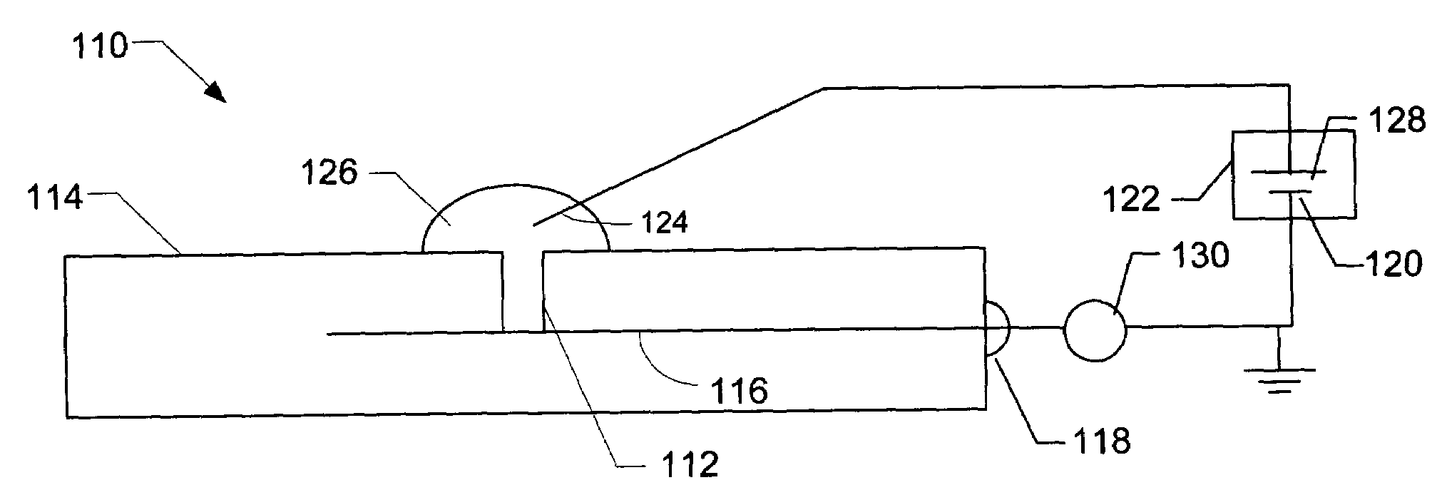
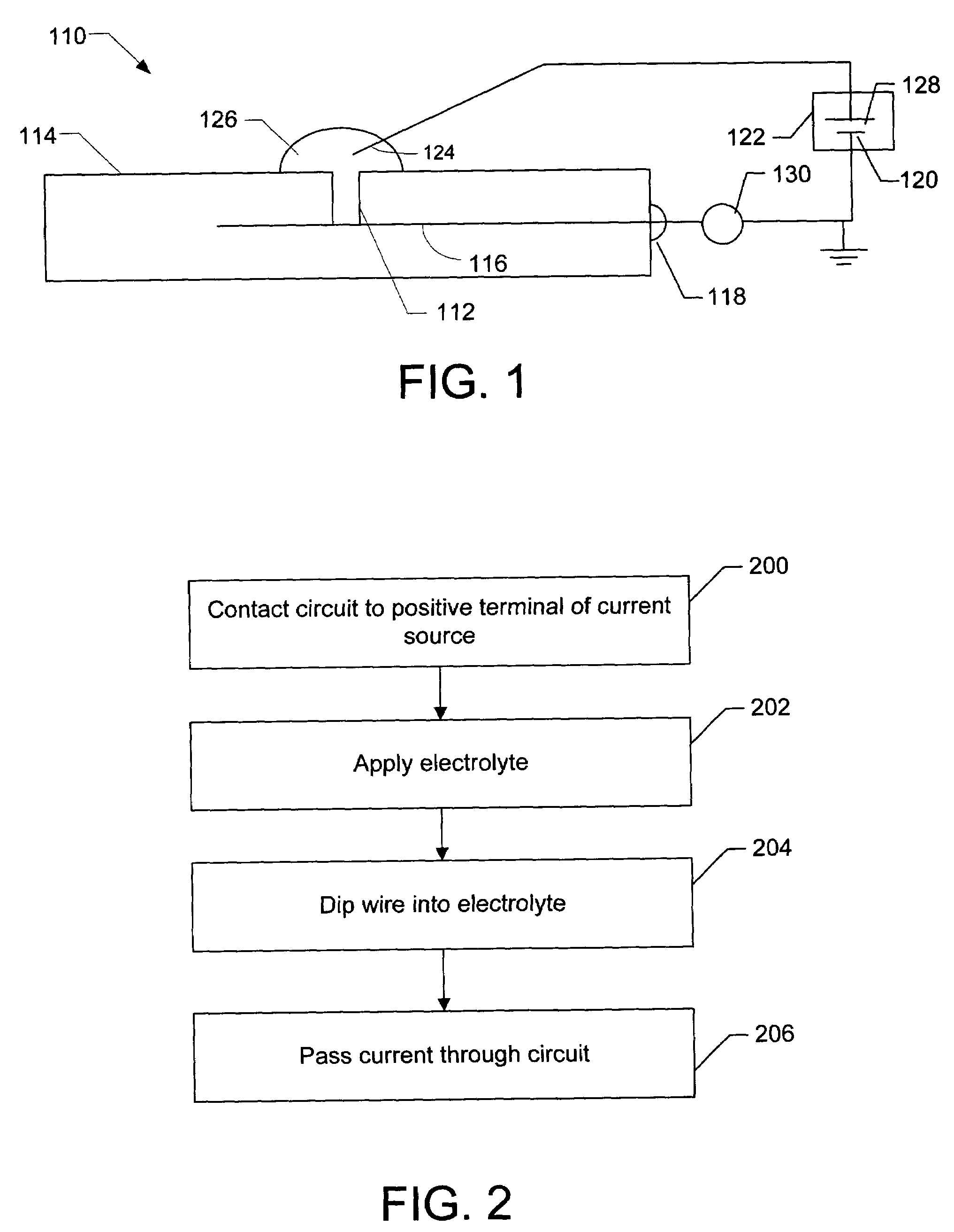
[0033]Several preferred embodiments of the invention are applicable to the field of “circuit editing,” that is, adding or removing electrical paths to change the connections in an integrated circuit by a heterogeneous electron charge transfer mechanism, such as electrodepositing or electroetching. In particular, the invention is useful for filling vias, severing metallic lines through high-aspect ratio vias, and rapidly creating conductive lines.

[0034]Some embodiments of the invention can be used to deposit metals that are substantially pure. Metals deposited in accordance with the invention can have resistivities that are forty or more times lower than the resistivities of existing FIB-deposited tungsten and platinum materials, and ten times lower than the resistivity of FIB-deposited copper conductive materials.

[0035]In some embodiments, the invention can be practiced in air, outside a vacuum chamber. In other embodiments, the invention can be practiced within a vacuum chamber use...


PUM

PropertyMeasurementUnit
diameteraaaaaaaaaa
diameteraaaaaaaaaa
depthaaaaaaaaaa

Abstract

A charge transfer mechanism is used to locally deposit or remove material for a small structure. A local electrochemical cell is created without having to immerse the entire work piece in a bath. The charge transfer mechanism can be used together with a charged particle beam or laser system to modify small structures, such as integrated circuits or micro-electromechanical system. The charge transfer process can be performed in air or, in some embodiments, in a vacuum chamber.

Description

[0001]This application claims priority from U.S. Provisional Pat. App. No. 60 / 561,701, which is hereby incorporated by reference.TECHNICAL FIELD OF THE INVENTION[0002]The present invention relates to modifying small structures and is particularly useful in the field of nanotechnology, such as in integrated circuit fabrication and repair.BACKGROUND OF THE INVENTION[0003]Semiconductor devices such as microprocessors can be made up of millions of transistors, each interconnected by thin metallic lines branching on several levels and electrically isolated from each other by layers of insulating materials. When a new semiconductor design is first produced in a semiconductor fabrication facility, the design typically does not operate exactly as expected. It is then necessary for the engineers who designed the device to review their design and “rewire” it to achieve the desired functionality. Due to the complexity of building a semiconductor device in a semiconductor fabrication facility, ...

Claims


Application Information

Patent Timeline
Patent Type & Authority Patents(United States)
IPC IPC(8): H01L21/4763H01L21/768H01L21/3205H01L23/52
CPCC25D5/02C25F3/12C25F3/14C25D3/665H01L21/32134H01L21/76892H01L21/76894H01L21/2885B42D25/29G06Q40/04
Inventor GU, GEORGE Y.BASSOM, NEIL J.GANNON, THOMAS J.LIU, KUN
Owner FEI CO
Why Eureka
Try Eureka