Charge control apparatus and measurement apparatus equipped with the charge control apparatus

a control apparatus and charge control technology, applied in the direction of instruments, nuclear engineering, and fault location by increasing destruction at fault, can solve the problems of inconvenient installation of observation means suitable for semiconductor inspection instruments, measurement accuracy may deteriorate, and measurement accuracy may be too large to be measured separately as a second electron source, etc., to achieve the effect of improving repeatability, high speed, and performing charge processing efficiently

Active Publication Date: 2010-03-23
HITACHI HIGH-TECH CORP
View PDF11 Cites 40 Cited by
  • Summary
  • Abstract
  • Description
  • Claims
  • Application Information

AI Technical Summary

Benefits of technology

[0010]In view of this, the present invention has an object to perform charge processing efficiently by observing an electrified state by predetermined observation means and feeding back observation results to a charged particle beam illumination system installed separately from the primary electron beam illumination system.
[0011]In order to solve the above-mentioned problem, in the charge control apparatus of this invention, electrons illuminating a specimen and the specimen are relatively moved so that ununiformity of charge resulting from variation of an emission current is reduced, and at the same time charge is monitored. The means for relatively moving electrons and the specimen is at least one means selected from among means for scanning an electron beam using a deflector, means for moving an electron source, and means for moving a specimen, or a combination of two or more means. The means for monitoring charge of a specimen is at least one means selected from among means for monitoring an absorption current flowing into the specimen, means for, when using an charge control electrode, monitoring an absorption current flowing into the electrode, and means for monitoring the secondary electrons emitted from the specimen and backscattered electrons, or a combination of two or more means. By the relative movement, arbitrary charge including 0 V can be given to the specimen uniformly and with high speed. Then, by applying the charge control apparatus of this invention to a measurement apparatus using charged particles, improvement in both measurement precision of the measurement apparatus and repeatability can be realized. Moreover, in the case where the charge control apparatus is applied to an inspection instrument for semiconductor using charged particles, high-sensitivity detection of a failure of electric characteristics can be realized.

Problems solved by technology

However, since generally surfaces of circuit patterns are constructed with an insulating film made of SiO2, SiN, a polymer, such as a resist, or the like, there is a problem that, if circuit patterns are measured using charged particles, such as an electron beam, surfaces of semiconductor devices are electrified and accordingly measurement precision may deteriorate.
In addition, in the inspection of semiconductor devices, there arise needs of inspection for failures of electric characteristics, such as conduction and non-conduction, that are difficult to detect with optical inspection instruments, and consequently electron beam type inspection instruments are coming into wide use.
They are too massive to install separately as a second electron source, and needs a lens etc. to irradiate a large area at one time.
However, observation means suitable for an inspection instrument of a semiconductor device did not exist conventionally.
In this case, since charge processing and potential measurement cannot be conducted simultaneously, whether charge of the surface by charge processing has reached saturation cannot be determined and hence determination as to whether charge processing is completed is impossible.
Therefore, it is unsuitable to apply this system to the semiconductor measurement apparatus that is required high-precision ad high-speed charge control.
Moreover, although JP-A No. 173528 / 2000 discloses a technology of detecting an electrified state by monitoring a variation in voltage contrast of an acquired image, it comes with a necessity of performing image processing each time an electrified state is analyzed, and consequently it does not match high-speed of processing.

Method used


Image

  • Charge control apparatus and measurement apparatus equipped with the charge control apparatus
  • Charge control apparatus and measurement apparatus equipped with the charge control apparatus
  • Charge control apparatus and measurement apparatus equipped with the charge control apparatus

Examples


first embodiment

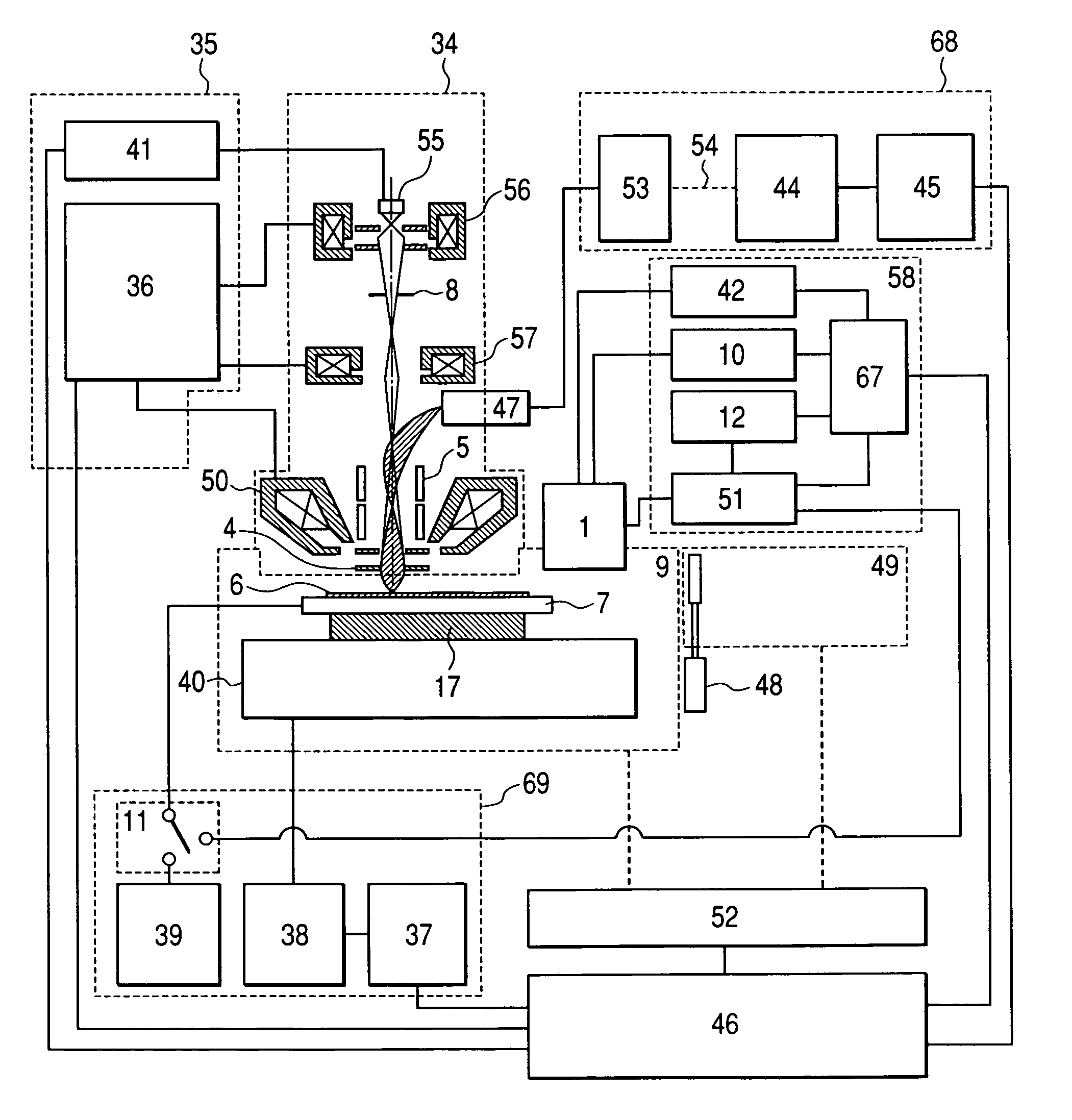
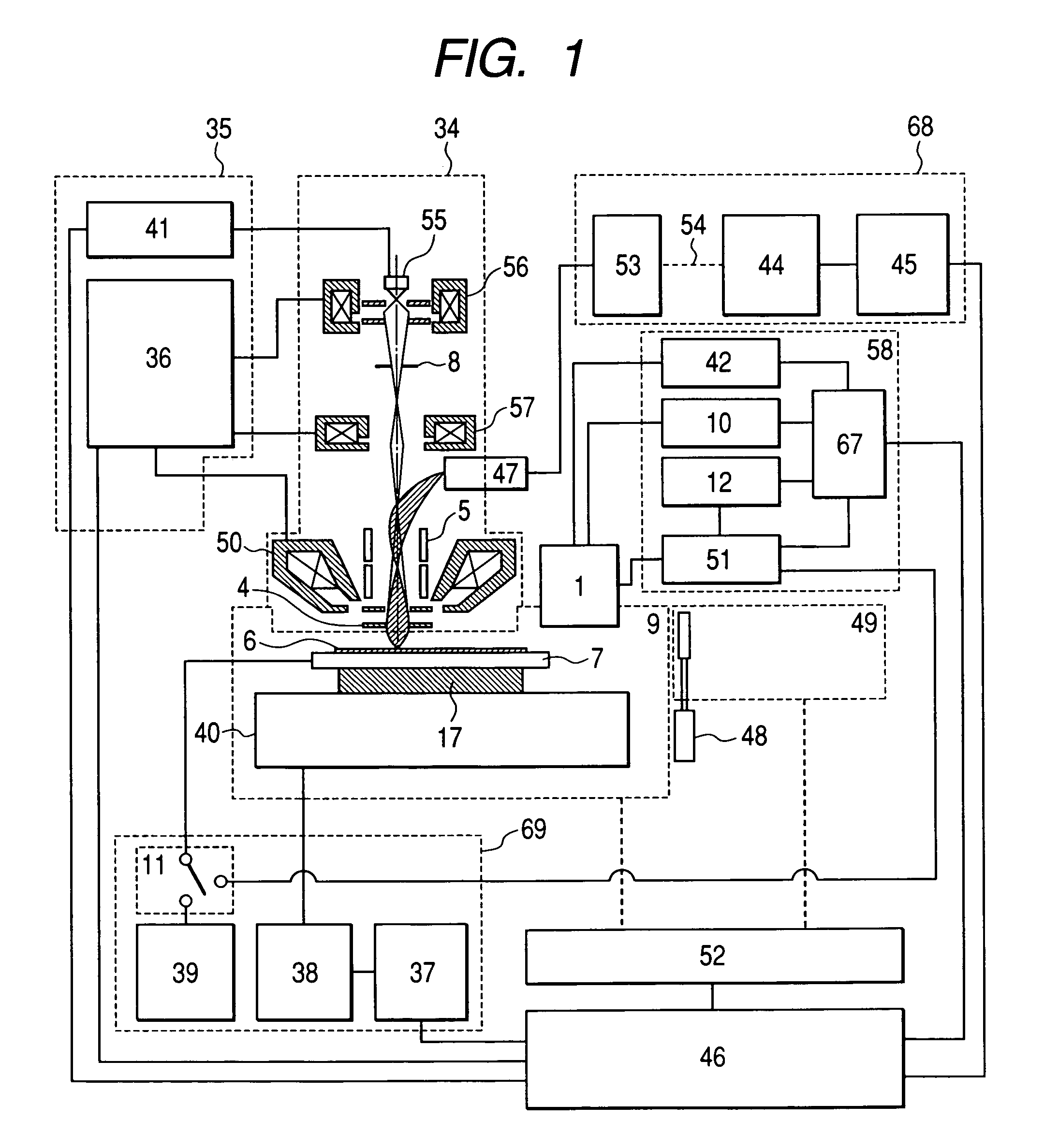
[0045]In this embodiment, an example of one configuration of an SEM type semiconductor inspection instrument to which charge processing technology is applied will be explained. The SEM type semiconductor inspection instrument explained in this embodiment has a configuration where a charged particle beam illumination system for charge control and an SEM column are arraigned in parallel to a specimen, having a feature that a charge control beam is irradiated perpendicularly on a semiconductor wafer that is an inspection target. Moreover, in this embodiment, especially an embodiment that uses a CNT cathode as a charged particle beam source for charge control will be explained.

[0046]For a charged particle beam source for charge control, an electron source capable of illuminating a large area with a large current and realizing stable emission is preferable. The CNT cathode can irradiate a large area at one time and operate without heating at a degree of vacuum of about 1×10⁻⁴ [Pa], and c...

second embodiment

[0081]In the electron beam application device shown in the first embodiment, charge on the specimen surface is controlled using the charge control column provided adjacent to the SEM column, uses both scanning of electrons and movement of the stage together, and renders charge uniform. In the second embodiment, the electron beam application instrument equipped with an charge control function in the specimen reparatory chamber was explained. Moreover, the charge control apparatus of this embodiment is different from the charge control apparatus explained in the first embodiment in that its operating principle is not charge control by the charge control electrode, charge on the specimen surface is controlled with incident energy of the primary electron beam that irradiates a specimen, and the charge control apparatus is relatively moved to the specimen to render charge uniform.

[0082]FIG. 9 shows an example of a semiconductor pattern inspection instrument with which the above-mentioned...

third embodiment

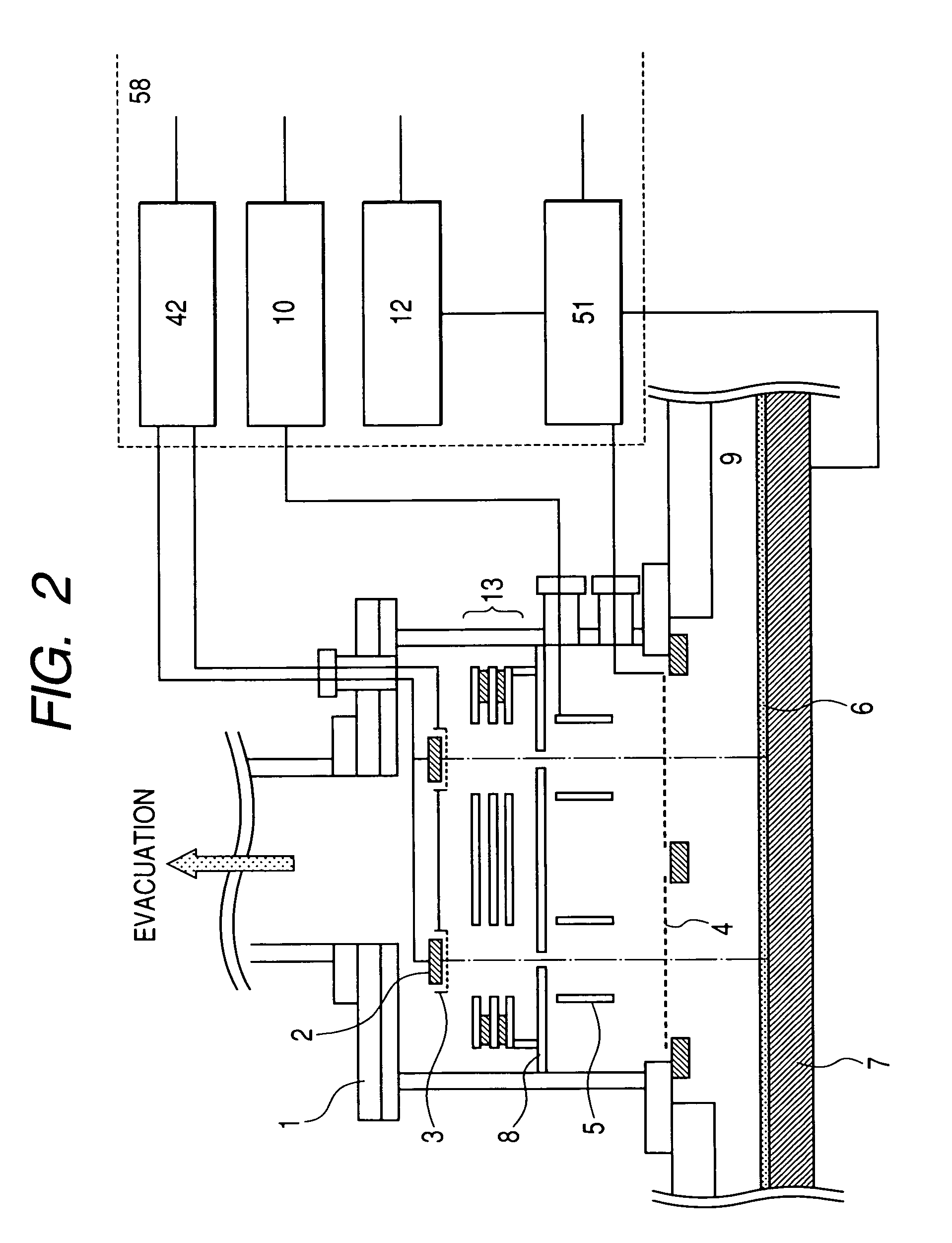
[0091]In the first Embodiment, an example of the SEM type semiconductor inspection instrument where the electron beam emitted from the electron gun for charge control is irradiated in parallel to the specimen was explained. In this embodiment, another example of configuration of the SEM type semiconductor inspection instrument will be described. A feature of the SEM type semiconductor inspection instrument of this embodiment is a capability to realize charge control processing by incorporating a small electron gun into the conventional SEM column. At this time, electron illumination is done by the electron gun, and charge processing for controlling the charge is performed by using an charge control electrode provided in the SEM column.

[0092]FIG. 13 shows a general view of the semiconductor inspection instrument of this embodiment. The semiconductor inspection instrument of this embodiment is roughly divided into: an SEM column 34, a charge control column 1, the specimen chamber 9, t...


PUM


Abstract

The invention solves charge nonuniformity of a specimen surface resulting from emission variation of a carbon nanotube electron source and individual difference of emission characteristics. During charge control processing, charge of the specimen surface is measured in real time. As means for solving charge nonuniformity resulting from nonuniformity of electron illumination density, electrons illuminating the specimen and the specimen are moved relatively to average electron illumination density. Moreover, an absorption current flowing into the specimen and the numbers of secondary electrons emitted from the specimen and of backscattered electrons are measured as means for monitoring charge of the specimen surface in real time.

Description

CLAIM OF PRIORITY[0001]The present application claims priority from Japanese application JP 2005-017596 filed on Jan. 26, 2005, and JP 2005-298311 filed on Oct. 13, 2005, the contents of which are hereby incorporated by reference into this application.FIELD OF THE INVENTION[0002]This invention relates to a measurement apparatus and a measurement method for controlling a potential of the surface of a specimen constructed with a pattern including an insulator on its surface, such as a semiconductor device and a liquid crystal device, and a measurement apparatus for a semiconductor device, a liquid crystal device, etc. having the charge control device (charge control apparatus) and a measuring method therefor.BACKGROUND OF THE INVENTION[0003]In these days, a technology of measuring a state of a circuit pattern formed on a wafer during a process assumes an important role in a manufacture line of a semiconductor device. Conventionally, most of these measuring technologies are ones that a...

Claims


Application Information

Patent Timeline
Patent Type & Authority Patents(United States)
IPC IPC(8): H01J37/256
CPCH01J37/026H01J37/073H01J37/28H01J2237/0048H01J2237/0635H01J2237/24564H01J2237/2594
Inventor MAKINO, HIROSHICHENG, ZHAOHUITANIMOTO, KENJITODOKORO, HIDEO
Owner HITACHI HIGH-TECH CORP
Why Eureka
Try Eureka