Apparatus and method for improving drive-strength and leakage of deep submicron MOS transistors

a technology drive strength, which is applied in the field of deep submicron mos transistor drive strength and leakage improvement, can solve the problems of a whopping 100 amperes of leakage current, relatively uncontrolled decrease of threshold voltage, and the user of conventional complementary metal-oxide semiconductor (cmos) technology, etc., to achieve improved drive strength, reduce leakage current, and improve the effect of area efficiency

Inactive Publication Date: 2010-03-23
SEMI SOLUTIONS LLC
View PDF76 Cites 44 Cited by
  • Summary
  • Abstract
  • Description
  • Claims
  • Application Information

AI Technical Summary

Benefits of technology

[0011]An apparatus and method of manufacture for metal-oxide semiconductor (MOS) transistors is disclosed. Devices in accordance with the invention are operable at voltages below 2V. The devices are area efficient, have improved drive strength, and have reduced leakage current. The inventive devices use a dynamic threshold voltage control scheme that is implemented without changing the existing MOS technology process. This scheme controls the threshold voltage of each transistor. In the OFF state, the magnitude of the threshold voltage of the transistor is increase, keeping the transistor leakage to a minimum. In the ON state, the magnitude of the threshold voltage is decreased, resulting in increased drive strength. The invention is particularly useful in MOS technology for both bulk and silicon on insulator (SOI) CMOS. The use of reverse biasing of the well, in conjunction with the above construct to further decrease leakage in a MOS transistor, is also shown.

Problems solved by technology

Users of conventional complementary metal-oxide semiconductor (CMOS) technology currently face some difficult choices as the minimum feature size of such devices shrinks to below 100 nanometers and power supply voltage is reduced to less than 1.0V.
Given a leakage of every gate of 1 microamperes, this results in a whopping 100 amperes of leakage current.
The accumulated holes cause a relatively uncontrolled decrease in threshold voltage.
The use of a backward biased diode is deficient in several ways.
Firstly, the reverse current through the diode varies over orders of magnitude and is highly sensitive to temperature.
Secondly, while Ebina deals effectively with voltage ranges of 2 volts and above, it fails to provide a solution for transistor operating in lower voltages as common in modern designs.
The area penalty is fairly large for this approach and it requires additional process steps.

Method used


Image

  • Apparatus and method for improving drive-strength and leakage of deep submicron MOS transistors
  • Apparatus and method for improving drive-strength and leakage of deep submicron MOS transistors
  • Apparatus and method for improving drive-strength and leakage of deep submicron MOS transistors

Examples


Embodiment Construction

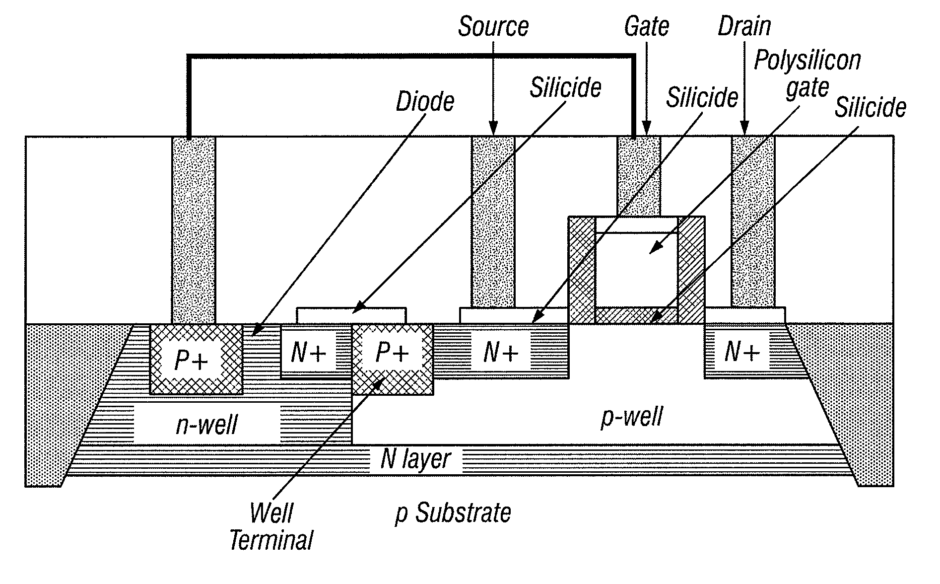
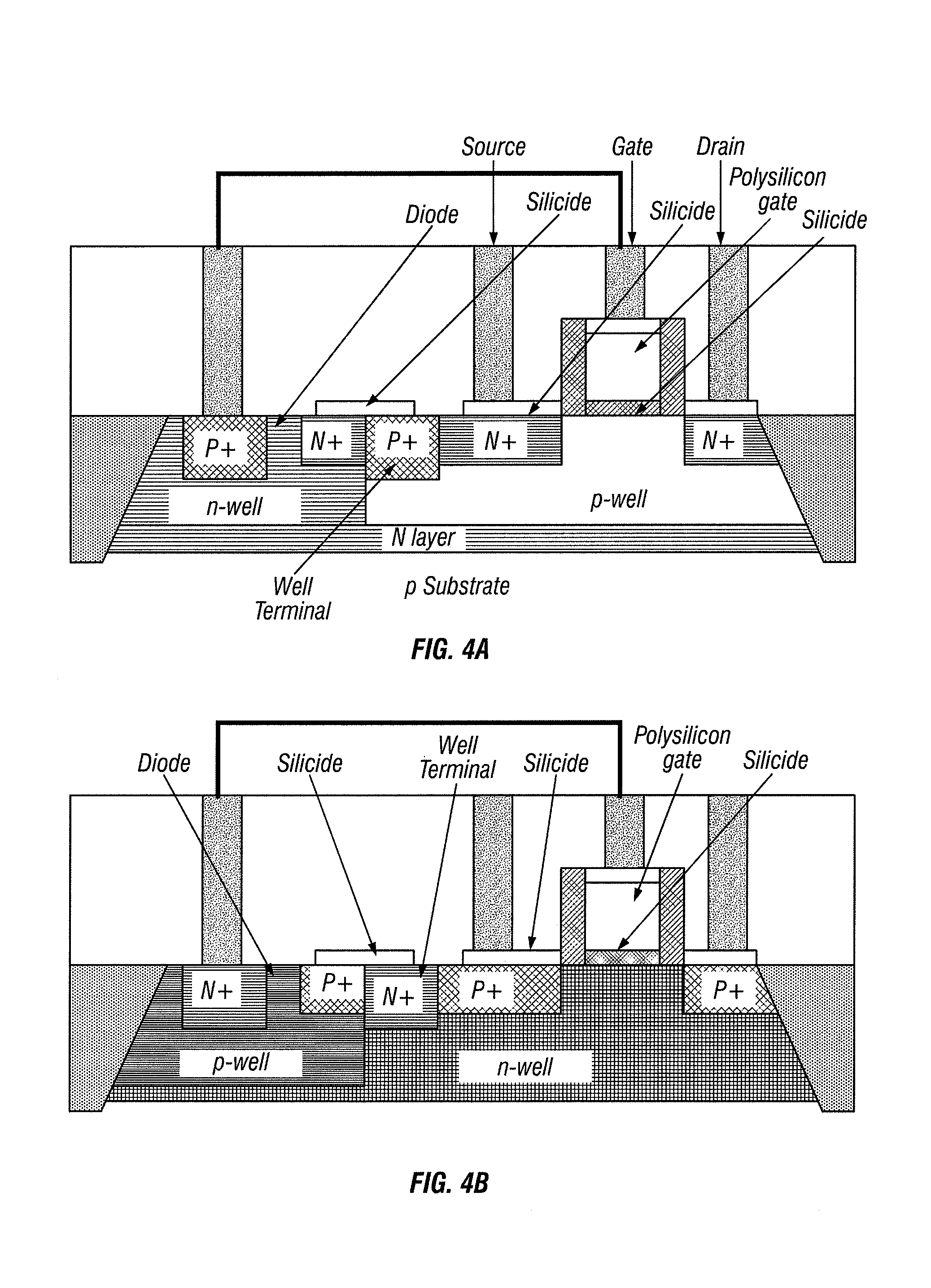
[0030]The invention comprises the addition of a circuit to a MOS transistor, for example an NMOS transistor, that results in an increase in drive current while the transistor is in an ON state, and a reduction in leakage current while the transistor is in the OFF state. Specifically, this is achieved by implementing a control circuit between the gate and the substrate or well of the transistor. The control circuit may be comprised of linear and / or non-linear passive components and can be as simple as a resistor, a capacitor, or include one or more diodes, in a plurality of combinations suitable for leakage current reduction. Specifically, the circuit forces a high threshold voltage VTH in the OFF state of the NMOS transistor and a low VTH in the ON state of the NMOS transistor. A person skilled in the art would note that such a control circuit would work equally well with a PMOS type transistor. A detailed description of the disclosed invention follows.

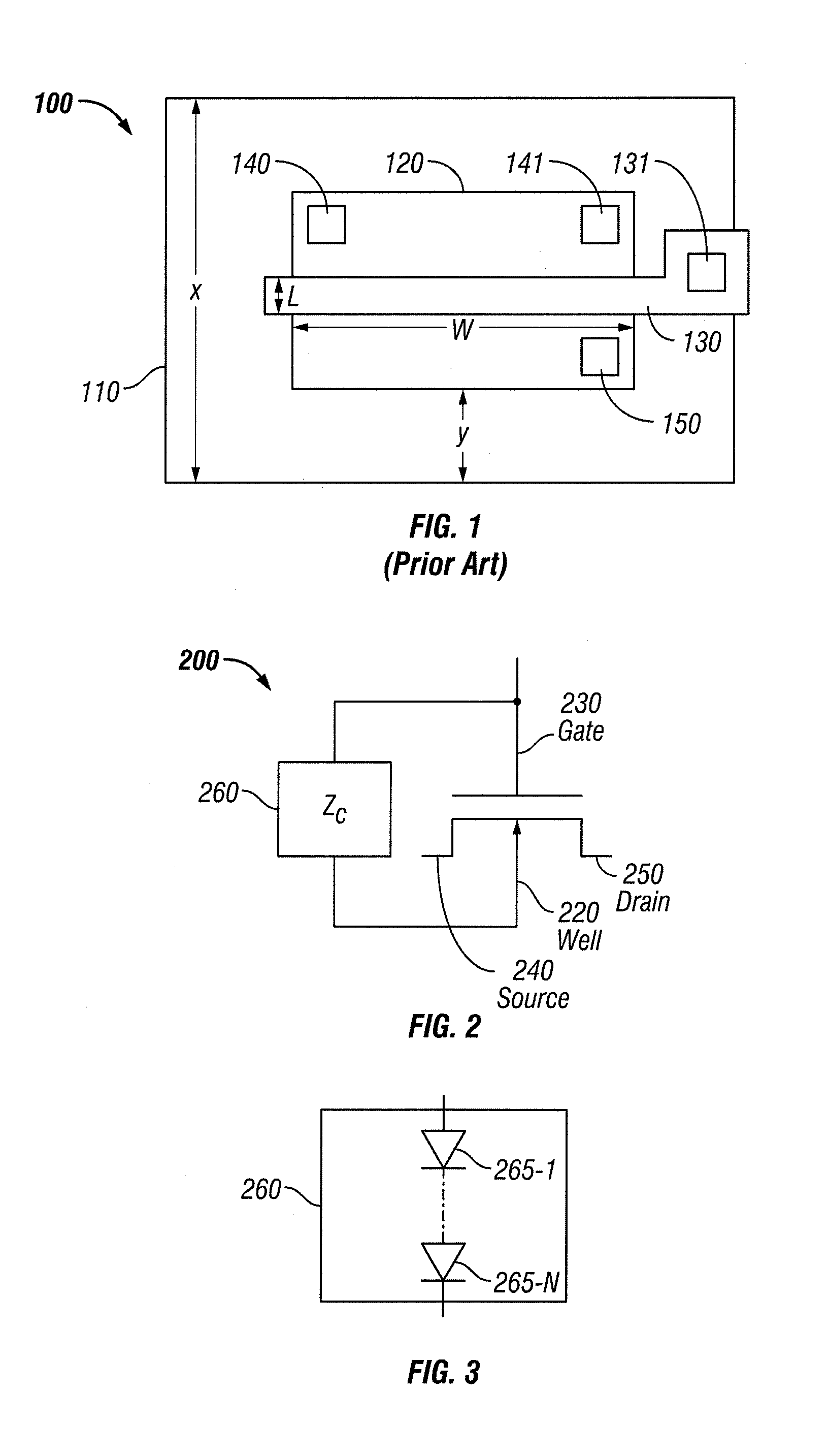
[0031]FIG. 2 is a schematic di...


PUM


Abstract

An apparatus and method of manufacture for metal-oxide semiconductor (MOS) transistors is disclosed. Devices in accordance with the invention are operable at voltages below 2V. The devices are area efficient, have improved drive strength, and have reduced leakage current. A dynamic threshold voltage control scheme comprised of a forward biased diode in parallel with a capacitor is used, implemented without changing the existing MOS technology process. This scheme controls the threshold voltage of each transistor. In the OFF state, the magnitude of the threshold voltage of the transistor increases, keeping the transistor leakage to a minimum. In the ON state, the magnitude of the threshold voltage decreases, resulting in increased drive strength. The invention is particularly useful in MOS technology for both bulk and silicon on insulator (SOI) CMOS. The use of reverse biasing of the well, in conjunction with the above construct to further decrease leakage in a MOS transistor, is also shown.

Description

CROSS REFERENCE TO RELATED APPLICATIONS[0001]This application is a continuation-in-part of U.S. patent application Ser. No. 11 / 029,542, filed Jan. 4, 2005 U.S. Pat. No. 7,224,205, the entirety of which is incorporated herein by this reference thereto. The application further claims priority from U.S. provisional patent application Ser. Nos. 60 / 717,769, filed Sep. 19, 2005, and 60 / 601,979 filed Aug. 17, 2004, and 60 / 585,582 filed Jul. 7, 2004.BACKGROUND OF THE INVENTION[0002]1. Technical Field[0003]The invention relates to MOS transistors. More specifically, the invention relates to the improvement of drive-strength and leakage of deep submicron MOS transistors.[0004]2. Discussion of the Prior Art[0005]Users of conventional complementary metal-oxide semiconductor (CMOS) technology currently face some difficult choices as the minimum feature size of such devices shrinks to below 100 nanometers and power supply voltage is reduced to less than 1.0V. A typical layout of a 0.18 micron tra...

Claims


Application Information

Patent Timeline
Patent Type & Authority Patents(United States)
IPC IPC(8): H01L29/76H01L31/062H01L31/113H01L31/119
CPCH01L27/0629H01L27/0727H01L29/78H03K19/0005H03K19/0016H03K19/00361H01L27/1203
Inventor KAPOOR, ASHOK KUMARSTRAIN, ROBERTMARKO, REUVEN
Owner SEMI SOLUTIONS LLC
Why Eureka
Try Eureka