

Dual-gate sensor
a dual-gate, sensor technology, applied in the field of sensors, can solve the problems of difficult to perform electrical measurement with high sensitivity, difficult to accurately perform electrical measurement, and the like, and achieve the effect of stable electrical property measurement and high detection accuracy
- Summary
- Abstract
- Description
- Claims
- Application Information
AI Technical Summary
Benefits of technology
Problems solved by technology
Method used
Image

Examples
example 1
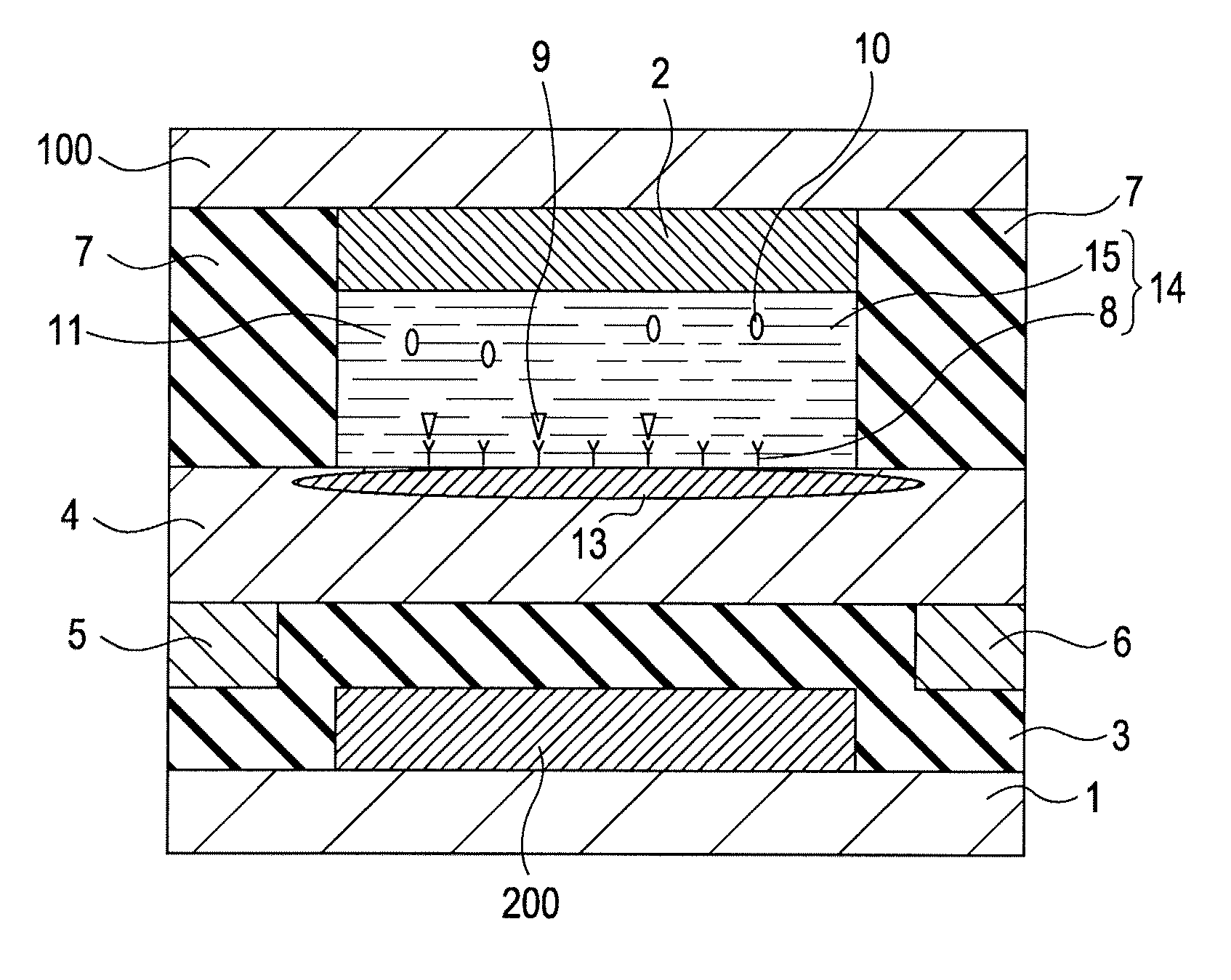
[0049]A dual-gate sensor shown in FIG. 3 is fabricated. Gold is vapor-deposited on a plastic substrate 1 to form a second gold gate electrode 200. A solution containing a polyimide is applied by spin-coating on the second gate electrode 200, followed by drying, to form a gate-insulating layer 3 with a thickness of 800 nm. Tetrabenzoporphyrin is vapor-deposited with a thickness of 70 nm on the gate-insulating layer 3, and carboxyl group-containing tetrabenzoporphyrin is vapor-deposited thereon with a thickness of 10 nm to form a semiconductor layer 4. Subsequently, gold is vapor-deposited on the resulting semiconductor layer 4 to form a source electrode 5 and a drain electrode 6 such that the gate length (distance between the source electrode and the drain electrode) is 50 μm and the gate width is 3 mm. Furthermore, in order to prevent the source electrode 5 and the drain electrode 6 from being in contact with a sample solution 10, an insulating film 7 made of parylene is formed.
[005...
PUM
 Abstract
Description
Claims
Application Information