Semiconductor laser diode

a laser diode and semiconductor technology, applied in semiconductor lasers, laser details, electrical equipment, etc., can solve the problems of reducing yield, disadvantageous low cod level, and inferior adhesiveness between the semiconductor interface and the dielectric film, so as to reduce the production yield and improve the heat radiability. , the effect of reducing the production yield

Active Publication Date: 2010-04-13
SHARP FUKUYAMA LASER CO LTD
View PDF9 Cites 2 Cited by
  • Summary
  • Abstract
  • Description
  • Claims
  • Application Information

AI Technical Summary

Benefits of technology

[0011]According to Patent Literature 2, the first dielectric film of Al2O3, the second dielectric film of Si3N4 or AlN and the third dielectric film of Al2O3 are stacked with each other so that the Al2O3 films protect the Si3N4 film inferior in chemical resistance by holding the same therebetween. However, the thermal expansion coefficient of the Si3N4 or AlN film is disadvantageously remarkably different from that of a GaAs-based material. When a film having a thickness of at least 50 nm is formed, therefore, film separation remarkably results from the difference between the thermal expansion coefficients of the first dielectric film of Al2O3 and the second dielectric film of SiN to disadvantageously reduce the production yield, regardless of film forming conditions.
[0014]The present invention has been proposed in order to solve the aforementioned problems, and an object of the present invention is to provide a semiconductor laser diode having sufficient initial characteristics, capable of stable high-output lasing over a long period with no reduction of a catastrophic optical damage level on an emission end through a film structure having excellent heat radiability.
[0016]According to the present invention, a semiconductor laser diode ensuring reliability by improving adhesiveness between a first dielectric film and a second dielectric film higher in thermal conductivity than the first dielectric film, preventing reduction of a COD level resulting from film separation or surface nitriding and suppressing deterioration of an emission end resulting from catastrophic optical damage caused upon a high-output operation over a long time can be implemented by providing a laminated structure of the first dielectric film of an oxide and the second dielectric film of an oxynitride on one (emission end) of a pair of cavity facets.

Problems solved by technology

The COD level of the semiconductor laser diode according to the aforementioned Patent Literature 1 is not more than 200 mW when the AlxOyNz film is directly formed, and this COD level is disadvantageously low as that of a laser diode of not more than 300 mW.
Therefore, adhesiveness between the semiconductor interface and the dielectric film is so inferior that the yield is reduced due to a problem such as film separation.
However, the thermal expansion coefficient of the Si3N4 or AlN film is disadvantageously remarkably different from that of a GaAs-based material.
When a film having a thickness of at least 50 nm is formed, therefore, film separation remarkably results from the difference between the thermal expansion coefficients of the first dielectric film of Al2O3 and the second dielectric film of SiN to disadvantageously reduce the production yield, regardless of film forming conditions.
Upon lasing over a long period, therefore, the temperature of the emission end rises to progress end oxidation, to disadvantageously result in formation of high-density surface levels, facilitation of light absorption and aged deterioration of the COD level.
In addition, stress is hardly reduced due to the difference between the thermal expansion coefficients of the materials forming the Al2O3 films and the AlN or SiN film, and it is difficult to thickly form the film having excellent heat radiability.
It is conceivable that none of the semiconductor laser diodes having the aforementioned structures can satisfy sufficient reliability and a sufficient COD level meeting marketing needs for a high-output laser diode.

Method used


Image

  • Semiconductor laser diode
  • Semiconductor laser diode
  • Semiconductor laser diode

Examples


example 1

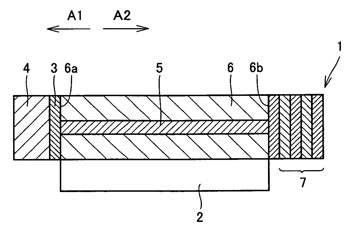
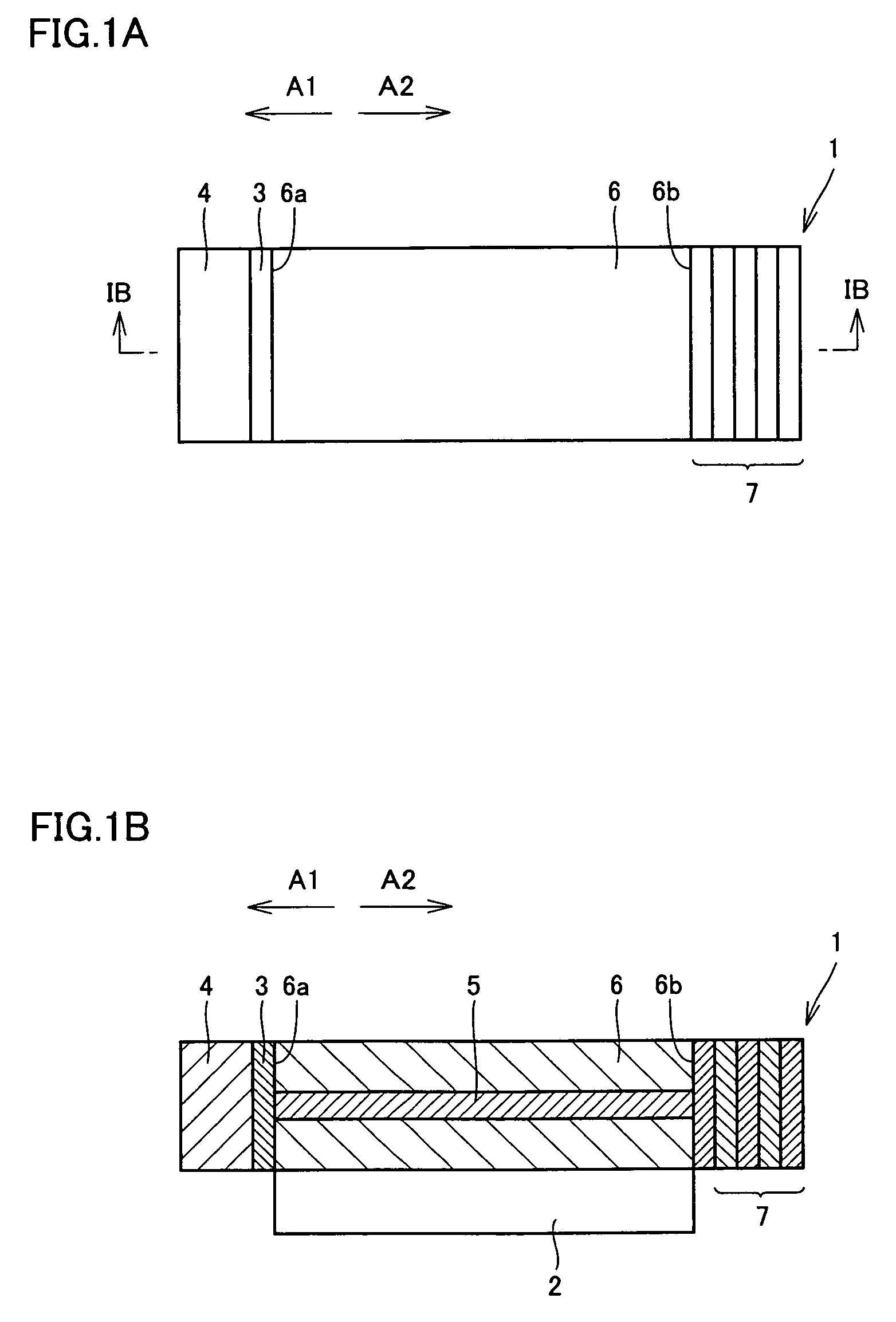
[0083]An n-type In0.5(Ga0.3Al0.7)0.5P cladding layer (n=3 to 4×1017 cm−3) having a thickness of 2.2 μm doped with Si, an active layer 5, a p-type In0.5(Ga0.3Al0.7)0.5P cladding layer (p=9×1017 cm−3) having a thickness of 1.5 μm doped with Zn, a p-type In0.5Ga0.5P energizable layer having a thickness of 50 nm doped with Zn and a p-type GaAs cap layer having a thickness of 0.5 μm doped with Zn were successively formed on an n-type GaAs substrate (semiconductor substrate) 2. Active layer 5 was formed by successively stacking an In0.5(Ga0.5Al0.5)0.5P first light guide layer having a thickness of 50 nm, an MQW active layer formed by an In0.65Ga0.35P well layer having a thickness of 5 nm and an In0.5(Ga0.5Al0.5)0.5P barrier layer having a thickness of 6 nm and an In0.5(Ga0.5Al0.5)0.5P second light guide layer having a thickness of 50 nm. These layers were formed by metal organic chemical vapor deposition (MOCVD).

[0084]Then, a striped resist material was formed on an end surface of a lamin...

example 2

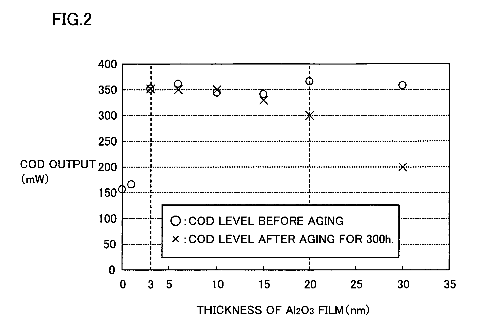
[0090]A semiconductor laser diode 1 according to Example 2 of the present invention similar to that according to the embodiment shown in FIGS. 1A and 1B was manufactured similarly to Example 1, except that first and second dielectric films 3 and 4 were prepared from Al2O3 (thickness: 6 nm) and AlxOyNz (thickness: 100 nm) respectively without formation of a third dielectric film. Reflectivity of this semiconductor laser diode measured similarly to Example 1 was 7%. The semiconductor laser diode according to Example 2 was also preferable as a red semiconductor laser diode of the 650 nm band.

example 3

[0091]A semiconductor laser diode 1′ according to Example 3 of the present invention similar to that according to the embodiment shown in FIG. 6 was manufactured similarly to Example 1, except that first, second and third dielectric films 3, 4 and8 were prepared from AlxOyNz (thickness: 20 nm) obtained by introducing 5% of nitrogen into Al2O3, AlxOyNz (thickness: 30 nm) having an oxygen content of 10% and SiO2 respectively. Reflectivity of this semiconductor laser diode measured similarly to Example 1 was 8%. The semiconductor laser diode according to Example 3 was also preferable as a red semiconductor laser diode of the 650 nm band.

[0092]In the semiconductor laser diode according to Example 3, thermal conductivity on an interface was more improved as compared with the semiconductor laser diodes according to Examples 1 and 2 due to first dielectric film 3 of AlxOyNz prepared by introducing 5% of nitrogen into Al2O3 and second dielectric film 4 of AlxOyNz having the oxygen content o...


PUM


Abstract

A semiconductor laser diode comprising a semiconductor substrate having an active layer with a pair of cavity facets opposed to each other on both ends of active layer as well as a first dielectric film of an oxide and a second dielectric film of an oxynitride successively stacked on one cavity facet has sufficient initial characteristics with a film structure having excellent heat radiability for allowing stable high-output lasing over a long period without reducing a catastrophic optical damage level on an emission end.

Description

[0001]This nonprovisional application is based on Japanese Patent Application No. 2006-021144 filed with the Japan Patent Office on Jan. 30, 2006, the entire contents of which are hereby incorporated by reference.BACKGROUND OF THE INVENTION[0002]1. Field of the Invention[0003]The present invention relates to an end emission type semiconductor laser diode, and more specifically, it relates to a semiconductor laser diode stably operating with a high output over a long time while suppressing aged deterioration of an emission end resulting from reduction of a catastrophic optical damage level.[0004]2. Description of the Background Art[0005]When the quantity of current injection is increased in an end emission type semiconductor laser diode of the 650 nm band or the 780 nm band in order to increase the light output, the light output is abruptly reduced to stop lasing. This phenomenon, resulting from catastrophic optical damage (hereinafter abbreviated as COD) to an emission end of the se...

Claims


Application Information

Patent Timeline
Patent Type & Authority Patents(United States)
IPC IPC(8): H01S5/00
CPCB82Y20/00H01S5/028H01S5/34326H01S5/0287H01S5/162H01S5/0282
Inventor SOGABE, RYUICHIKAWAGUCHI, YOSHINOBUKAMIKAWA, TAKESHI
Owner SHARP FUKUYAMA LASER CO LTD
Why Eureka
Try Eureka