Electro-optical apparatus, electronic apparatus, and method of manufacturing electro-optical apparatus

a technology of electrooptical apparatus and electronic equipment, applied in the field of electromechanical equipment, can solve the problems of inability to realize high-speed operation in the gate line driving circuit or the source line driving circuit, too low current etc., to achieve the effect of the capacitance value per unit area, increasing the thickness, and improving the current characteristics of the thin-film transistor

Active Publication Date: 2010-04-27
JAPAN DISPLAY WEST
View PDF18 Cites 29 Cited by
  • Summary
  • Abstract
  • Description
  • Claims
  • Application Information

AI Technical Summary

Benefits of technology

[0007]An advantage of the invention is that it provides an electro-optical apparatus, which can have a gate insulating layer of increased thickness in one kind of thin-film transistor and another kind of thin-film transistor with improved ON current characteristics even when methods of manufacturing the two kinds of thin-film transistors are the same, an electronic apparatus including the electro-optical apparatus, and a method of manufacturing the electro-optical apparatus.
[0008]An advantage of the invention is that it provides an electro-optical apparatus, in which a variation in electric characteristics or deterioration of reliability does not occur in a thin-film transistor even when ON current characteristics of the thin-film transistor are improved, an electronic apparatus including the electro-optical apparatus, and a method of manufacturing the electro-optical apparatus.
[0009]An advantage of the invention is that it provides an electro-optical apparatus, which is capable of simultaneously improving ON current characteristics of a thin-film transistor and a capacitance value per unit area of a storage capacitor, an electronic apparatus including the electro-optical apparatus, and a method of manufacturing the electro-optical apparatus.
[0010]An advantage of the invention is that it provides an electro-optical apparatus, which is capable of simultaneously improving ON current characteristics of a thin-film transistor and efficiency of the electric connection to a lower conductive layer below a gate insulating layer, an electronic apparatus including the electro-optical apparatus, and a method of manufacturing the electro-optical apparatus.
[0011]According to an aspect of the invention, there is provided an electro-optical apparatus including a first thin-film transistor having a first gate electrode, a first gate insulating layer and a first active layer, which are respectively formed of a conductive film, an insulating film and a semiconductor film, in a pixel region of a device substrate, the apparatus including: a second thin-film transistor having a first gate electrode formed of the conductive film, a second gate insulating layer formed by removing a portion of the insulating film in a thickness direction and a second active layer formed of the semiconductor film, in a region other than the pixel region of the device substrate.
[0012]According to another aspect of the invention, there is provided a method of manufacturing an electro-optical apparatus including a first thin-film transistor having a first gate electrode, a first gate insulating layer and a first active layer in a pixel region of a device substrate and a second thin-film transistor having a second gate electrode, a second gate insulating layer and a second active layer in a region other than the pixel region of the device substrate, the method including: simultaneously forming the first gate electrode and the second gate electrode; forming the first gate insulating layer and the second gate insulating layer; forming the first active layer and the second active layer; and thinning an insulating film which overlaps the second gate electrode at an upper layer side by etching to reduce the thickness of the second gate insulating layer to be smaller than that of the first gate insulating layer.

Problems solved by technology

However, when the active layer 7g of the thin-film transistor 1g used in the driving circuit is formed using an amorphous silicon film similar to the active layer 7a of the thin-film transistor 1c, ON current is too low compared with a case of using a polysilicon film and thus a high-speed operation in the gate line driving circuit or the source line driving circuit cannot be realized.
Thus, the ON current of the thin-film transistor 1g is too low to be used in the driving circuit.
When the semiconductor film for configuring the active layer is formed of the amorphous silicon film, ON current is small and thus cannot be used in a driving circuit.
By this configuration, when the contact hole for connecting the lower conductive layer is formed, the insulating film which covers the lower conductive layer is thin and thus an etching time necessary for forming the contact hole for connecting the lower conductive layer is short.

Method used


Image

  • Electro-optical apparatus, electronic apparatus, and method of manufacturing electro-optical apparatus
  • Electro-optical apparatus, electronic apparatus, and method of manufacturing electro-optical apparatus
  • Electro-optical apparatus, electronic apparatus, and method of manufacturing electro-optical apparatus

Examples


embodiment 1

Configuration of Liquid Crystal Apparatus

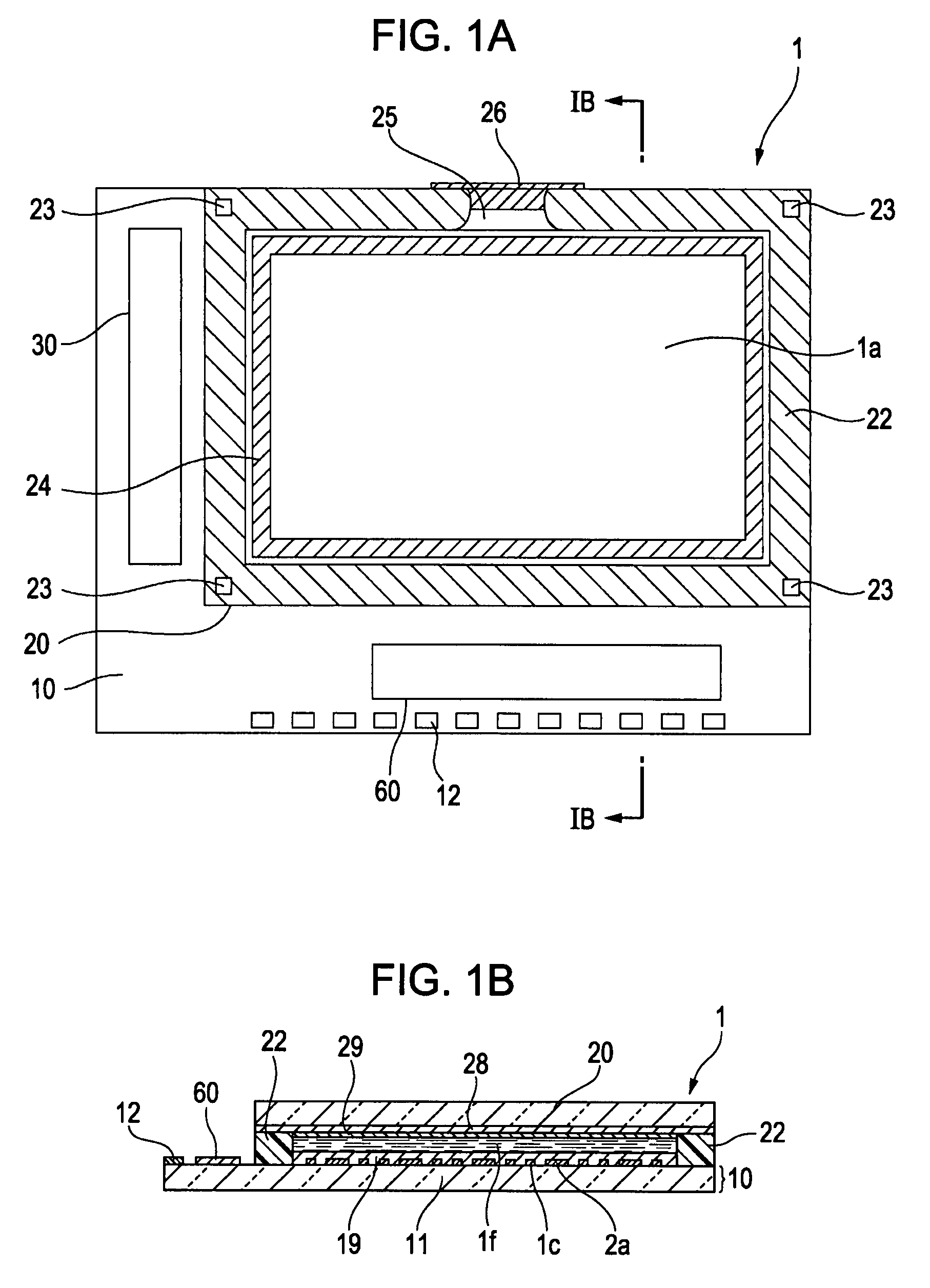
[0048]FIGS. 1a and 1b are respectively a plan view of a liquid crystal apparatus (electro-optical apparatus) together with components formed thereon when viewed from a counter substrate and a cross-sectional view taken along line 1B-1B. The liquid crystal apparatus 1 according to the present embodiment is a transmissive active-matrix liquid crystal display apparatus of a twisted nematic (TN) mode, an electrically controlled birefringence (ECB) mode or a vertical aligned nematic (VAN) mode. In the liquid crystal apparatus 1, a device substrate 10 and a counter substrate 20 are adhered through a seal material 22 and liquid crystal 1f is held therebetween as an electro-optical material.

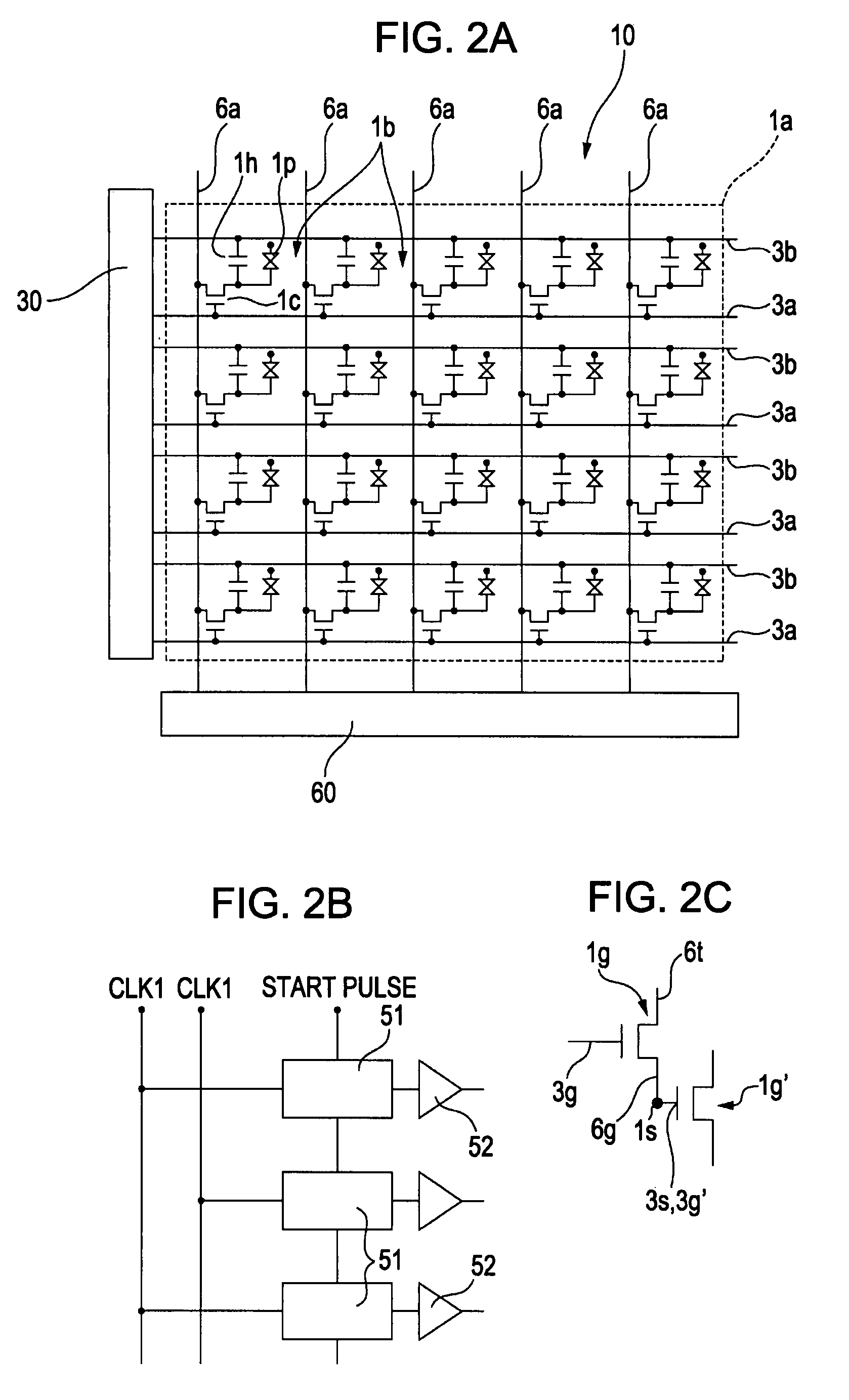
[0049]In the present embodiment, as described below, an active layer of thin-film transistors formed on the device substrate 10 is formed of an amorphous silicon film. As shown in FIGS. 1a and 1b, on the device substrate 10, a data line driving circuit 60 and a sc...

modified example 1 of embodiment 1

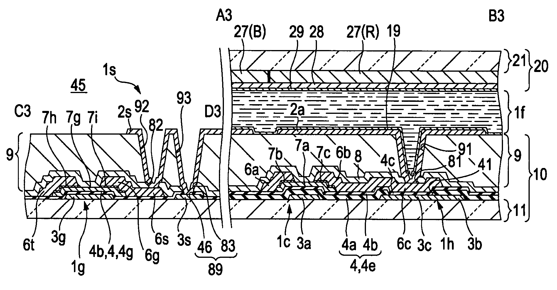
[0097]Although, in Embodiment 1, the upper hole 83 of the contact hole 89 is formed in the process of forming the contact hole shown in FIG. 6c and the insulating film 4 (the upper insulating film 4b) located at the bottom of the upper hole 83 is removed to form the lower hole 46 in the other etching process, when the thicknesses of the upper electrode 6c and the upper conductive layer 6s are large and the thickness of the insulating film 4 in which the contact hole 89 for connecting the lower conductive layer is formed is small, the contact holes 81, 82 and 89 may simultaneously formed in the process of forming the contact holes. The present embodiment is not limited to Embodiment 1 and is applicable to the following embodiments.

modified example 2 of embodiment 1

[0098]Although, in Embodiment 1, the removed region 45 in which the lower insulating film 4a is removed over the thickness direction is formed over the wide region of the driving circuit forming region of FIGS. 3b and 3c, the removed region 45 in which the lower insulating film 4a is removed over the thickness direction may be formed in the inner region spaced apart from the outer edge of a region, in which the signal line 3g and the active layer 7g overlap, by a predetermined distance, as shown in FIGS. 7b and 7c, similar to a region in which the storage capacitor 1h is formed as shown in FIGS. 7a and 7b. By this configuration, since the thick insulating film 4 can be interposed in the outer edge of the region in which the signal line 3g and the active layer 7g overlap, it is possible to ensure a sufficient gate withstanding voltage of the thin-film transistor 1g even when the gate insulating layer 4g is thinned. At this time, in the contact portion 1s, the remove region 45 in whic...


PUM


Abstract

Provided is an electro-optical apparatus including a first thin-film transistor having a first gate electrode, a first gate insulating layer and a first active layer, which are respectively formed of a conductive film, an insulating film and a semiconductor film, in a pixel region of a device substrate, the apparatus including: a second thin-film transistor having a first gate electrode formed of the conductive film, a second gate insulating layer formed by removing a portion of the insulating film in a thickness direction and a second active layer formed of the semiconductor film, in a region other than the pixel region of the device substrate.

Description

BACKGROUND[0001]1. Technical Field[0002]The present invention relates to an electro-optical apparatus, an electronic apparatus including thin-film transistors on a device substrate, and a method of manufacturing the electro-optical apparatus.[0003]2. Related Art[0004]Among a variety of electro-optical apparatuses, in an active matrix liquid crystal apparatus, for example, liquid crystal is held between a device substrate 10 shown in FIGS. 19a and 19b and a counter substrate (not shown). In the device substrate 10, a pixel-switching thin-film transistor 1c and a pixel electrode 2a electrically connected to a drain of the thin-film transistor 1c is formed in each of a plurality of pixel regions 1e corresponding to intersections between gate lines 3a (scanning lines) and source lines 6a (data lines). The alignment of molecules of the liquid crystal is controlled by an image signal applied to the pixel electrode 2a from the source line 6a through the thin-film transistor 1c in each pixe...

Claims


Application Information

Patent Timeline
Patent Type & Authority Patents(United States)
IPC IPC(8): H01L21/20H01L29/00
CPCG02F1/13454H01L27/1255H01L29/4908
Inventor SATO, TAKASHI
Owner JAPAN DISPLAY WEST
Why Eureka
Try Eureka