ESD structure

a technology of electrostatic discharge and structure, applied in the direction of semiconductor devices, semiconductor/solid-state device details, electrical apparatus, etc., can solve the problems of several defects produced during locos processing, weak oxide growth over the region of the region, and the edge of the isolation of defects, etc., to achieve more robust esd performance

Active Publication Date: 2010-05-04
INTERSIL INC
View PDF11 Cites 0 Cited by
  • Summary
  • Abstract
  • Description
  • Claims
  • Application Information

AI Technical Summary

Benefits of technology

[0002]The present disclosure relates generally to electrostatic discharge (ESD) protection and, more specifically, to an improved transistor for use in an ESD circuit. The improved transistor will also provide a more robust ESD performance when used in circuitry not directly related to ESD protection.
[0010]The present IGFET minimizes the effect of the dislocation at the edge of the device region by displacing the lateral edges of the source and drain regions from the adjacent edge of the opening and the dislocation. This minimizes the lateral diffusion of the source and drain impurities and the formation of metal silicides into the dislocation region. The spacing of the lateral edges of the source and drain regions from the adjacent edge of the opening and the dislocation region is produced by providing additional lateral opposed second gate regions or oxide barrier layer extending from the oxide layer into the adjacent regions of the substrate region and the first gate region extending therebetween. Both the first gate region and the two second gate regions or barrier layer are used in the self-aligned processing of the source and drain regions. The first gate region defines the length of the channel, while the two opposed second gate regions or barrier layer define the width of the channel region. The second gate portion or barrier extends sufficiently into the substrate region to space the width of the channel from the adjacent edge of the opening in the oxide.

Problems solved by technology

For processes that use LOCOS (localized oxidation of silicon), shallow or deep trench isolation and other methods to define active device regions, defects occur at the edge of the isolation.
There are several defects that are produced during LOCOS processing.
A “white ribbon” occurs when the silicon near the bird's beak 18 becomes nitrified and results in a weakness in the oxide growing over that region during subsequent processing.
It is very difficult to completely remove this stress-related defect.
Likewise for other types of device isolation such as deep or shallow trench, there are stress-related and processing-related defects.
This is an undesirable effect.
This is caused by the silicide processing that can cause the silicide to ‘decorate’ the defect.

Method used


Image

  • ESD structure
  • ESD structure
  • ESD structure

Examples


Embodiment Construction

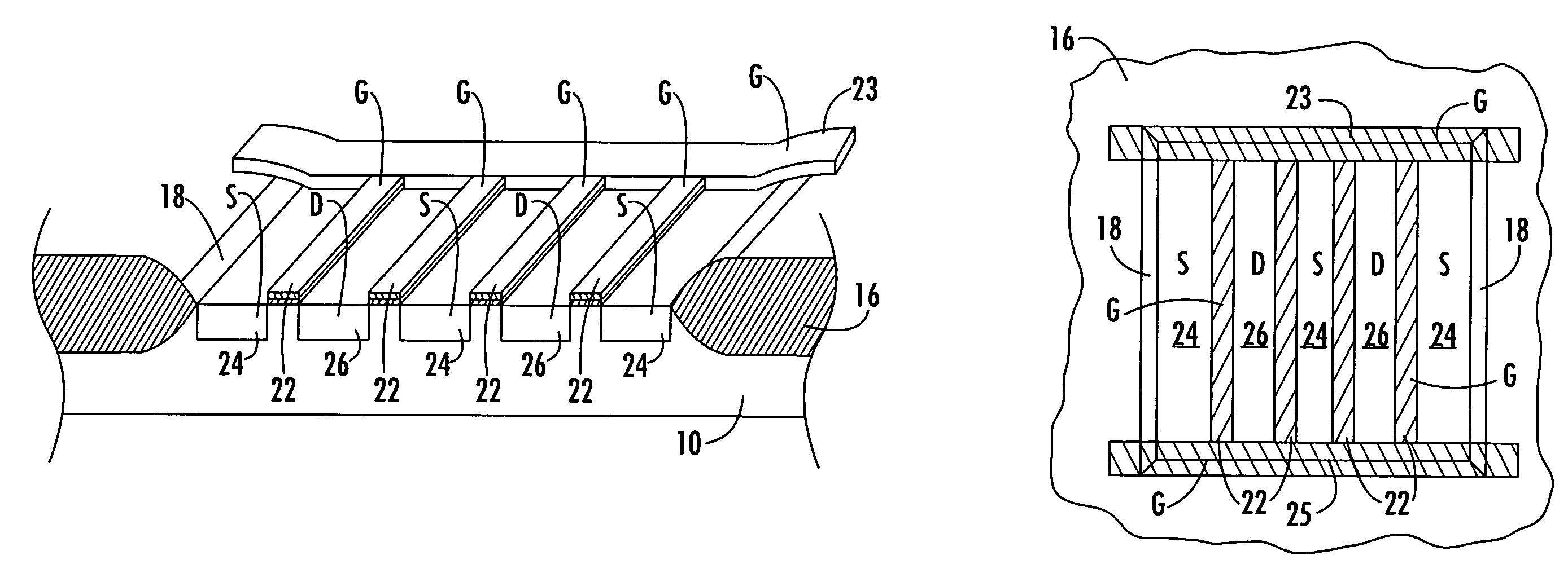
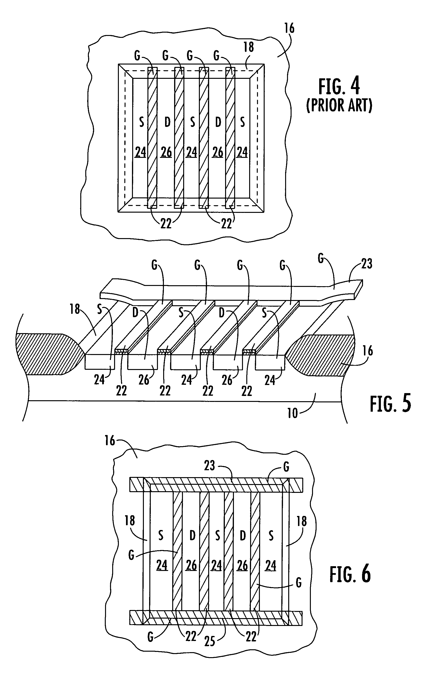
[0027]An IGFET, according to the present disclosure, having a similar structure as that shown in FIG. 4 is illustrated in FIGS. 5 and 6. A plurality of first gate portions 22 lie on an insulative layer 21 in the device region 20 and separates a plurality of sources 24 and drains 26. A pair of opposed second gate portions 23, 25 extend from the LOCOS 16 over the bird's beak 18 onto the device region 20 of the substrate 10. The first gate portion 22 extends between the second gate portions 23, 25. The source regions 24 and the drain regions 26 have their lateral edges displaced from the edge of the device region 20, LOCOS 16 and bird's beak 18. The gate material may be polycrystalline silicon, for example.

[0028]The device of FIGS. 5 and 6 are produced using a self-aligned gate technique. By using the gate portions 22, 23, 25 in the self-alignment process, the first gate portion 22 defines the length of the channel regions 28, while the opposed gate regions 23, 25 define the width of t...


PUM


Abstract

An IGFET that minimizes the effect of the dislocation at the edge of the device region by displacing the lateral edges of the source and drain regions from the adjacent edge of the opening and the dislocation. This minimizes the lateral diffusion of the source and drain impurities and the formation of metal silicides into the dislocation region. The spacing of the lateral edges of the source and drain regions from the adjacent edge of the opening and the dislocation region is produced by providing additional lateral opposed second gate regions or oxide barrier layer extending from the oxide layer into the adjacent regions of the substrate region and the first gate region extending therebetween. Both the first gate region and the two second gate regions or barrier layer are used in the self-aligned processing of the source and drain regions. The first gate region defines the length of the channel, while the two opposed second gate regions or barrier layer define the width of the channel region. The second gate portion or barrier extends sufficiently into the substrate region to space the width of the channel from the adjacent edge of the opening in the oxide.

Description

CROSS REFERENCE[0001]The present application claims the benefit of provisional U.S. application Ser. No. 60 / 625,584 filed Nov. 8, 2004 and Ser. No. 60 / 693,435 filed Jun. 24, 2005, which are incorporated herein by reference.BACKGROUND AND SUMMARY OF THE DISCLOSURE[0002]The present disclosure relates generally to electrostatic discharge (ESD) protection and, more specifically, to an improved transistor for use in an ESD circuit. The improved transistor will also provide a more robust ESD performance when used in circuitry not directly related to ESD protection.[0003]For processes that use LOCOS (localized oxidation of silicon), shallow or deep trench isolation and other methods to define active device regions, defects occur at the edge of the isolation. As illustrated in FIG. 1 where LOCOS isolation is used as an example, a substrate 10 has a nitride mask 14 separated from the surface of the substrate 10 by an oxide layer 12. The substrate 10 is subject to an oxidizing atmosphere, and...

Claims


Application Information

Patent Timeline
Patent Type & Authority Patents(United States)
IPC IPC(8): H01L27/088
CPCH01L29/78H01L27/0251
Inventor GAUL, STEPHEN JOSEPHCHURCH, MICHAEL D.VINSON, JAMES EDWIN
Owner INTERSIL INC
Why Eureka
Try Eureka