Plasma processing apparatus with insulated gas inlet pore

a technology of processing apparatus and gas inlet pore, which is applied in the direction of coatings, chemical vapor deposition coatings, electric discharge tubes, etc., can solve the problems of reducing the reliability of semiconductor parts, corroding inner parts of piping, and reducing yield, so as to prevent a decline in yield and reduce cost performance , the effect of increasing the frequency of piping replacemen

Active Publication Date: 2010-05-11
ASM JAPAN
View PDF3 Cites 286 Cited by
  • Summary
  • Abstract
  • Description
  • Claims
  • Application Information

AI Technical Summary

Benefits of technology

[0006]Such contamination not only remarkably lowers the reliability of semiconductor parts but also reduces throughput, which leads to manufacturing cost increase. Additionally, plasma discharge occurring inside the piping deteriorates the inside of the piping. By this, frequency of piping replacement increases and cost performance decreases. Further, throughput of semiconductor products is lowered.
[0007]Consequently, the present invention is intended to solve at least one of the problems, and an objection of the present invention, which is not intended to limit the present invention, is to provide a plasma processing apparatus which can suppress generation of plasma discharge inside the gas inlet piping and the gas inlet pore and prevent adhering of contaminants.
[0010]The insulation member is configured to suppress a potential voltage difference which would occur between the at least one of the electrodes and an inner wall of the gas inlet pipe at the gas inlet pore without the presence of the insulation member when radio-frequency power is applied to the electrodes.
[0020]The inner wall of the gas inlet pipe may be insulated from an edge connected to the inner periphery of the insulator to a point away from the edge by a distance effective to suppress an occurrence of plasma discharge at the gas inlet pore.
[0022]According to one or more embodiments of the present invention, one or more of the problems can be solved by suppressing plasma discharge inside the gas inlet piping and the gas inlet pore, thereby preventing adhering of products to an inner wall of the gas inlet piping and the gas inlet pore and a deterioration in the upper electrode by a plasma from becoming the source of contamination. As a result, in at least one embodiment, it becomes possible to prevent a decline in yield, increase in piping replacement frequency, a lowering of cost performance, and a drop in throughput of semiconductor products.
[0023]Further, in at least one embodiment, it becomes possible to suppress arc which would occur between the upper electrode and a wall of the reaction chamber when AC current flows between the upper and lower electrodes (DC bias voltage, Vdc, between the upper and lower electrodes can be maintained at minus values).

Problems solved by technology

As a result, a product adheres to an inner side of the gas inlet piping and the gas inlet pore, exfoliates, passes through the showerhead, and becomes the source of contamination.
Additionally, inner parts of the piping corrode by plasma discharge, from which metal powder is generated and becomes the source of contamination.
Such contamination not only remarkably lowers the reliability of semiconductor parts but also reduces throughput, which leads to manufacturing cost increase.
Additionally, plasma discharge occurring inside the piping deteriorates the inside of the piping.
By this, frequency of piping replacement increases and cost performance decreases.

Method used


Image

  • Plasma processing apparatus with insulated gas inlet pore
  • Plasma processing apparatus with insulated gas inlet pore
  • Plasma processing apparatus with insulated gas inlet pore

Examples


examples

[0051]The present invention will be explained with reference to the following examples. However, the examples are not intended to limit the present invention.

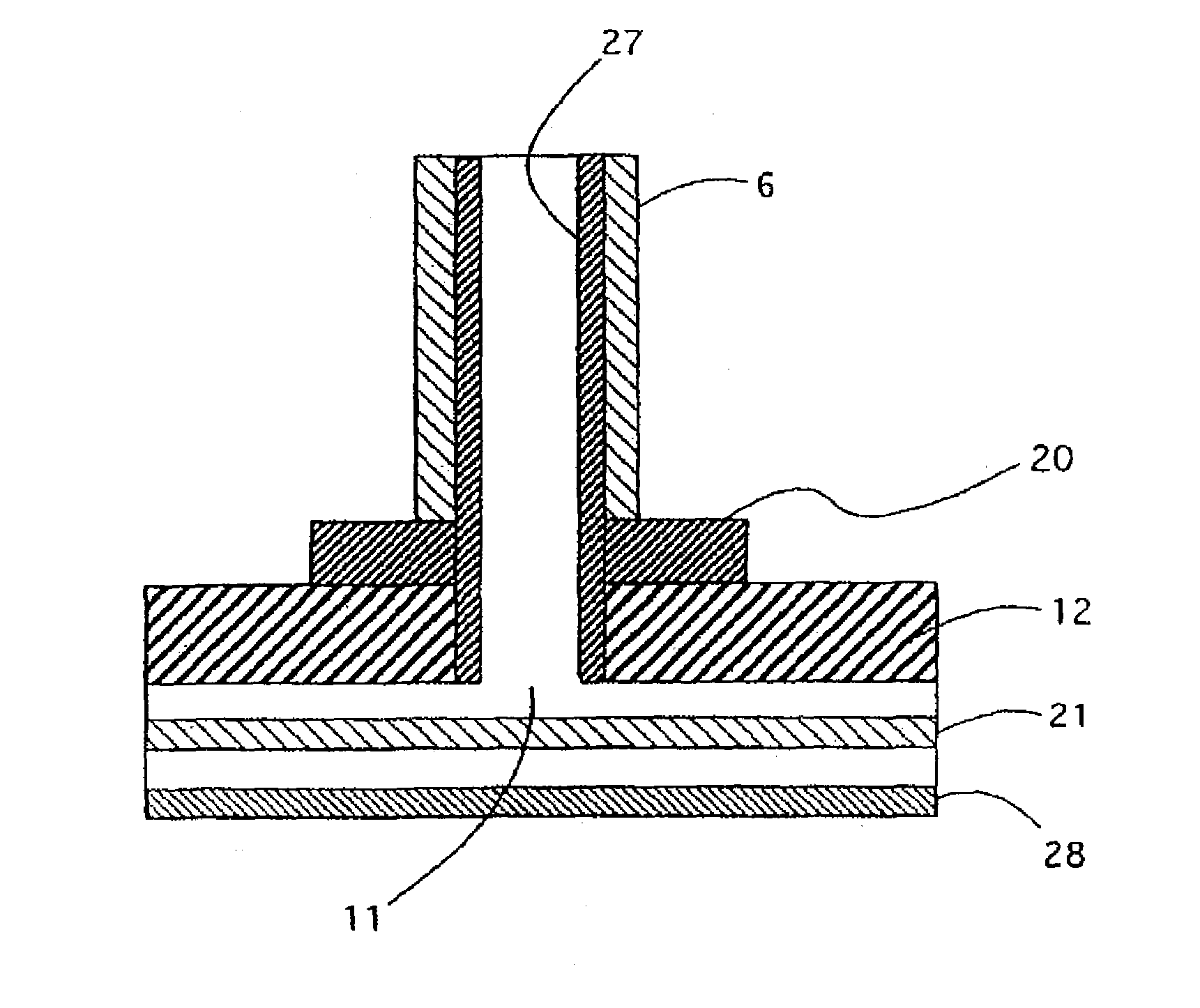
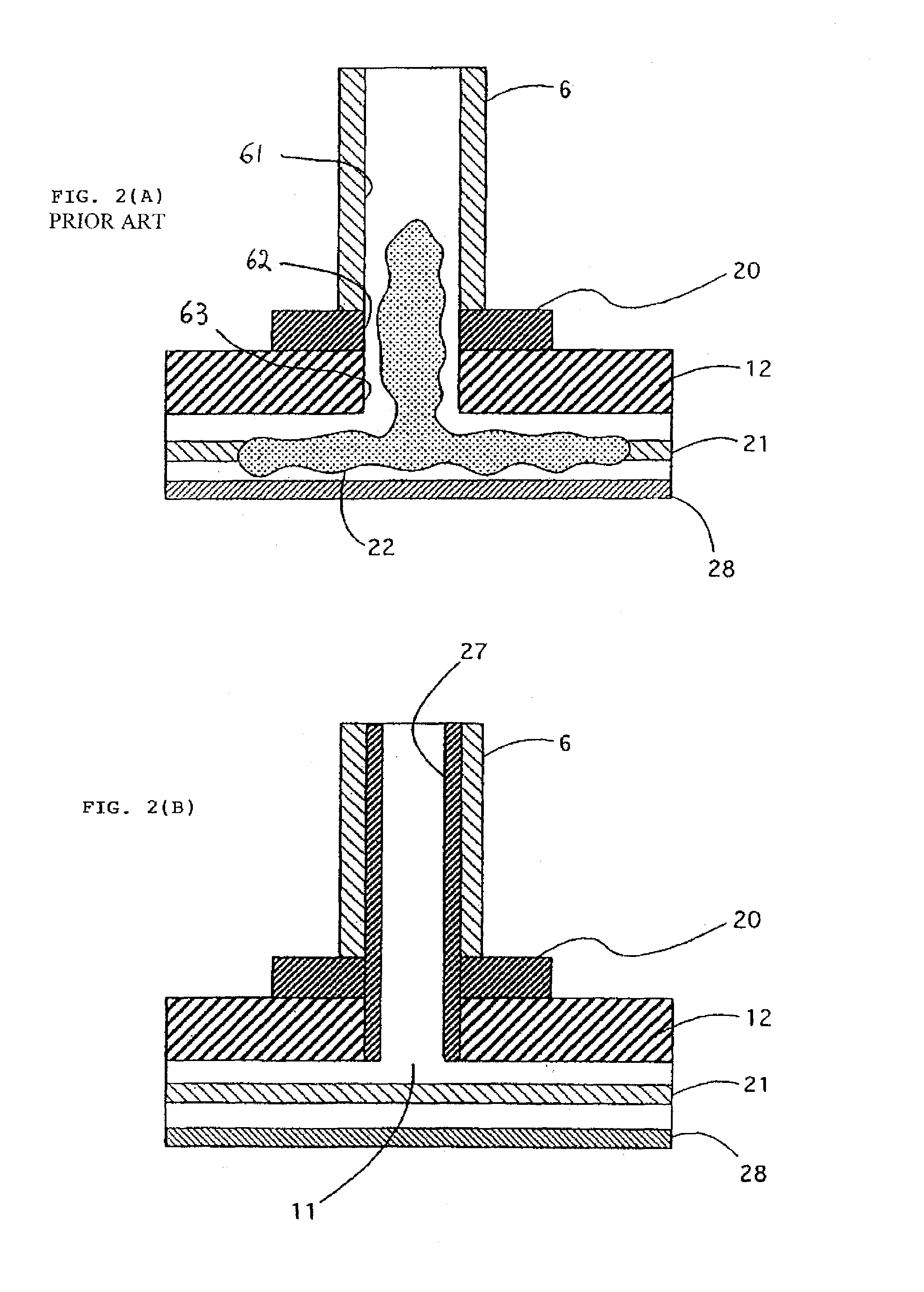
[0052]Thin-film formation experiments were conducted using a conventional plasma CVD apparatus and a plasma CVD apparatus according to an embodiment of the present invention (FIG. 2(B)). The tubular insulation was installed inside the a gas passage inner surface constituted by the inner wall 61 of the gas inlet piping 6, the inner periphery 62 of the ring-shaped insulator 20, and the inner periphery 63 of the gas inlet pore 11. The tubular insulator 27 had a radial thickness of 20 mm, an axial thickness (length) of 200 mm, and an inner diameter of 40 mm. In this case, the tubular insulator 27 covered a vertical portion of the gas inlet piping 6 in its entirety. The tubular insulator was made of aluminum oxide or magnesium oxide.

[0053]In the experiments, an oxygen-doped silicon carbide film and a nitrogen-doped silicon carbide f...


PUM

PropertyMeasurementUnit
thicknessaaaaaaaaaa
thicknessaaaaaaaaaa
thicknessaaaaaaaaaa

Abstract

A plasma processing apparatus includes: a reaction chamber; two electrodes provided inside the reaction chamber for generating a plasma therebetween, wherein at least one of the electrodes has at least one gas inlet pore through which a gas is introduced into the reaction chamber; and a gas inlet pipe coupled to the gas inlet pore for introducing the gas into the reaction chamber. The gas inlet pipe is grounded and insulated from the gas inlet pore, wherein an insulation member is placed inside the gas inlet pipe and the gas inlet pore.

Description

BACKGROUND OF THE INVENTION[0001]1. Field of the Invention[0002]The present invention generally relates to a plasma processing apparatus and particularly to a plasma processing apparatus having at least one gas inlet pore provided in electrodes for forming a thin film on a semiconductor substrate.[0003]2. Description of the Related Art[0004]Conventionally in the field of semiconductor device manufacturing, plasma processing such as plasma CVD and dry etching is frequently used. Generally, a plasma processing apparatus includes an evacuated reaction chamber, a susceptor installed inside the reaction chamber for placing a semiconductor substrate thereon, and a showerhead installed facing and parallel to the susceptor inside the reaction chamber. The susceptor is grounded and forms one side of electrodes for plasma discharge; the showerhead is connected to a radio-frequency power source provided outside the reaction chamber and forms the other side of the electrodes for plasma discharg...

Claims


Application Information

Patent Timeline
Patent Type & Authority Patents(United States)
IPC IPC(8): C23C16/507C23C16/50H01L21/306C23C16/509C23F1/00C23C16/06C23C16/22
CPCC23C16/325C23C16/5096H01J37/32559H01J37/3244H01J37/32091
Inventor YOSHIZAKI, YUNAKANO, RYU
Owner ASM JAPAN
Why Eureka
Try Eureka