
Aluminum thick film composition(s), electrode(s), semiconductor device(s) and methods of making thereof

a thin film composition and aluminum technology, applied in the direction of non-metal conductors, light radiation electric generators, conductors, etc., can solve the problems of insufficient inhibition, reduction in deformation or bowing, inability to address, etc., to reduce the electrical performance of fired solar cells, reduce the tendency of aluminum dusting, and reduce the bowing tendency

Inactive Publication Date: 2010-05-18
EI DU PONT DE NEMOURS & CO
View PDF31 Cites 25 Cited by
  • Summary
  • Abstract
  • Description
  • Claims
  • Application Information

AI Technical Summary

Benefits of technology

The present invention is about a thick film conductor composition that is used to make a p-type electrode for solar cells. The composition includes aluminum powder, amorphous silicon dioxide, and optional glass frit. The addition of amorphous silicon dioxide helps reduce bowing of the solar cells, while the optional glass frit helps reduce dusting. The invention also includes a process for making a solar cell by screen-printing the back-side of a silicon substrate with the composition and firing it at a specific temperature. The technical effect of this invention is to improve the efficiency and reliability of solar cells.

Problems solved by technology

Watsuji et al. further discloses that “[i]f the content of the inorganic compound powder is less than 0.3 mass percent, it is not possible to sufficiently inhibit the fired p-type silicon semi-conductor substrate from being deformed by adding the inorganic compound powder.” Additionally, the reduction in deformation or bowing as disclosed in Watsuji et al, is inadequate to address the requirements of cell manufacturers using back plane aluminum and module makers seeking to use current wafer thickness of less than 240 microns in a size of greater than 125 mm (5 inches) square where increased and costly breakage rates during production handling are observed when the bowing is greater than 1.5 mm.

Method used


Image

  • Aluminum thick film composition(s), electrode(s), semiconductor device(s) and methods of making thereof
  • Aluminum thick film composition(s), electrode(s), semiconductor device(s) and methods of making thereof
  • Aluminum thick film composition(s), electrode(s), semiconductor device(s) and methods of making thereof

Examples


examples

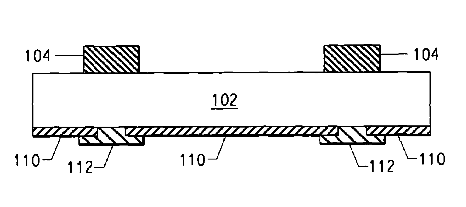
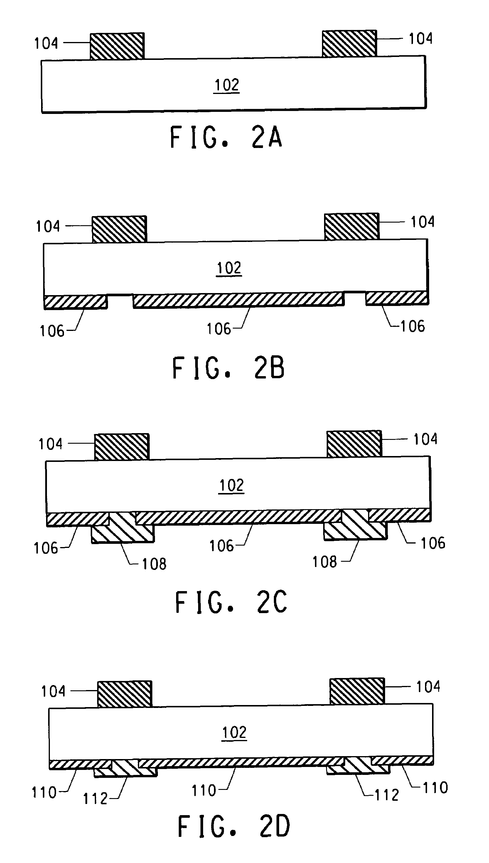
[0065]The examples cited here are based on firing said example pastes on wafers that have silicon nitride anti-reflection coating and are conventional cell designs with a front side n-type contact thick film silver paste. The performance of the paste is defined in terms of the electrical properties and additionally the bowing of the cell after firing (defined as the deflection of the fired cell at room temperature and the distance traveled at the centre of the wafer to achieve a flat cell).

[0066](1) Aluminum Paste With Finely Divided Amorphous Silicon Dioxide

[0067]Mixtures of aluminum powders with silicon dioxide are described here. It is known from U.S. Patent Publication 2004 / 0003836 that the relative silicon dioxide content with respect to the aluminum powder content and particle size affects electrical properties and extent of bowing of thinner cells to the lower level of 0.3 weight %. In the examples B and C cited in Table 1, we confirm that if crystalline silicon dioxide is ad...


PUM

PropertyMeasurementUnit
weight percentaaaaaaaaaa
thicknessaaaaaaaaaa
thicknessaaaaaaaaaa

Abstract

The present invention is directed to a thick film conductor composition comprised of (a) aluminum-containing powder; (b) amorphous silicon dioxide (c) and one or more optional glass frit compositions; dispersed in (d) organic medium. The amorphous silicon dioxide contributes to significant bow reduction tendency for solar cells thinner than 270 microns and larger than five inches square without significant effect on reducing the electrical performance of the fired solar cell. In addition and as preferred by solar cell manufacturers, the addition of glass frit reduces the dusting tendency of the aluminum thick film composition.

Description

FIELD OF THE INVENTION[0001]The present invention is directed primarily to thick film compositions, electrodes, and semiconductor devices. It is further directed to a silicon semiconductor device. In particular, it pertains to an electroconductive composition used in the formation of a thick film electrode of a solar cell.BACKGROUND OF THE INVENTION[0002]The present invention can be applied to a broad range of semiconductor devices, although it is especially effective in light-receiving elements such as photodiodes and solar cells. The background of the invention is described below with reference to solar cells, as a specific example of the prior art.[0003]A conventional solar cell structure with a p-type base has a negative electrode that is typically on the front-side or sun side of the cell and a positive electrode on the back-side. It is well known that radiation of an appropriate wavelength falling on a p-n junction of a semiconductor body serves as a source of external energy ...

Claims


Application Information

Patent Timeline
Patent Type & Authority Patents(United States)
IPC IPC(8): H01B1/22H01L31/00H02N6/00
CPCH01B1/24H01L31/022425Y02E10/50H05K1/092H01B1/20H01B1/22
Inventor ROSE, MICHAELYOUNG, RICHARD JOHN SHEFFIELD
Owner EI DU PONT DE NEMOURS & CO
Learn More