Package substrate and method for fabricating the same

a technology of packaging substrates and substrates, applied in the field of packaging substrates, can solve the problems of high cost, insufficient thickness, and inability to bond, and achieve the effects of enhancing bonding capability, strong texture, and high density wiring

Active Publication Date: 2010-05-18
PHOENIX PRECISION TECH CORP
View PDF5 Cites 12 Cited by
  • Summary
  • Abstract
  • Description
  • Claims
  • Application Information

AI Technical Summary

Benefits of technology

[0013]In view of the disadvantages of the prior art mentioned above, it is a primary objective of the present invention to provide a package substrate and a method for fabricating the same, which are capable of providing high density wiring and fine spacing between wire bonding pads.
[0014]It is another object of the present invention to provide a package substrate and a method for fabricating the same, which are capable of enhancing bonding capability with wire of wire bonding process and being advantageous to application demands of high number of pins.
[0025]The package substrate and a method for fabricating the same of the present invention mainly have a first insulating passivation layer and a second insulating passivation layer formed on the die attaching side and the ball implanting side of the substrate body respectively, and then sequentially form a chemical plating metal layer and wire bonding metal layer of plating gold on the wire bonding pads, therefore, the wire bonding pads have thicker gold layer thereon than the solder ball pads that has gold from chemical plating metal layer only; beside, plating gold has firmer texture than chemical plating gold, thereby enhancing bonding capability with wires of subsequent wire bonding process; accordingly, the first two fabrication method of the present invention avoid wiring process of plating lines and thus provide application demands of high density wiring and fine spacing.

Problems solved by technology

As stated above, chemical deposition is applicable to forming wire bonding metal layer 22 on the wire bonding pads 201, however, a sufficient thickness of wire bonding metal layer 22 costs highly, also wire bonding metal layer 22 formed by means of chemical deposition has softer texture and has poor bonding capability with wire of subsequent wire bonding process, thereby being disadvantageous to application demands of high number of pins.
However, the fabrication method is complicated and the cost is still high.
Besides, the insulating passivation layer 35, which is formed after the wire bonding metal layer 34 has been formed, causes contamination to the wire bonding metal layer 34 readily, thereby resulting in unstable quality of the subsequent wire bonding.

Method used


Image

  • Package substrate and method for fabricating the same
  • Package substrate and method for fabricating the same
  • Package substrate and method for fabricating the same

Examples


first embodiment

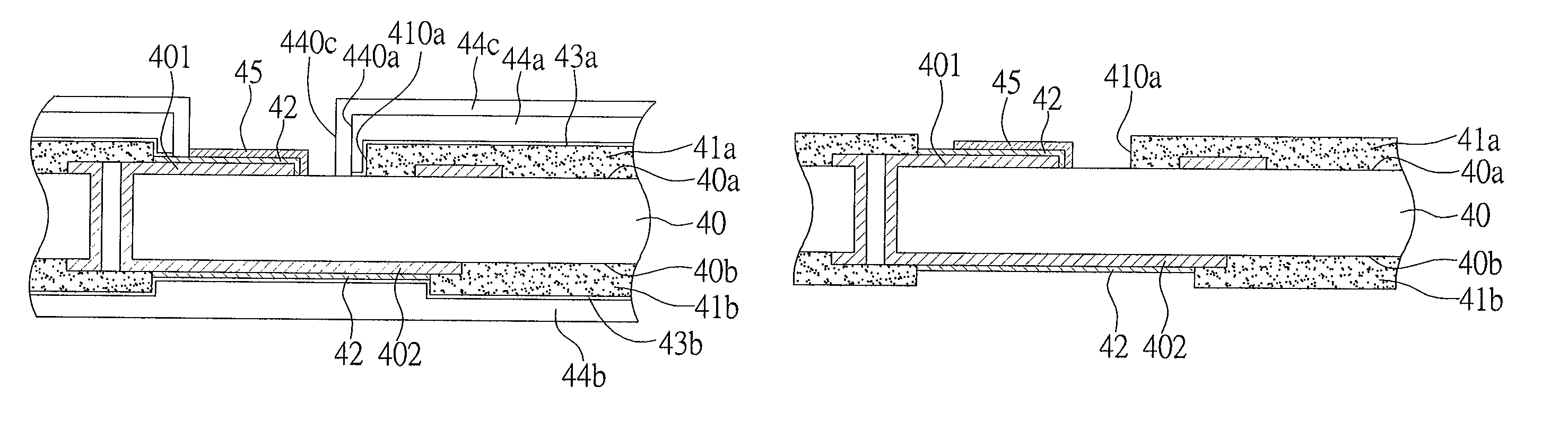
[0040]Please refer to FIGS. 4A through 4G, which are cross-sectional views illustrating the first embodiment of fabrication method of package substrate of the present invention.

[0041]As shown in FIG. 4A, provide a substrate body 40 with a die attaching side 40a and a ball implanting side 40b opposite each other, the die attaching side 40a and the ball implanting side 40b have a plurality of wire bonding pads 401 and a plurality of solder ball pads 402 respectively; form a first insulating passivation layer 41a and a second insulating passivation layer 41b on the die attaching side 40a and the ball implanting side 40b respectively, and then form a plurality of first apertures 410a and a plurality of second apertures 410b in the first insulating passivation layer 41a and the second insulating passivation layer 41b respectively to correspondingly expose the wire bonding pads and the solder ball pads. There are various related techniques for fabricating substrate bodies, the related tec...

second embodiment

[0048]Please refer to FIGS. 5A through 5E, which are cross-sectional views of the second embodiment of fabrication method of package substrate of the present invention.

[0049]As shown in FIGS. 5A and 5A′, provide first a structure as previously illustrated by FIG. 4C of the first embodiment, and then form a first photoresist layer 44a on the first conductive layer 43a, and also form a plurality of first openings 440a in the first photoresist layer 44a to correspondingly expose the first conductive layer 43a on area of the wire bonding pads 401, and the first openings 440a are smaller than the first apertures 410a of the first insulating passivation layer 41a to consequently cover part of the first conductive layer 43a on the wire bonding pads 401; and as shown in FIG. 5A, form a second photoresist layer 44b on the second conductive layer 43b, or, in accordance with structure illustrated by foregoing FIG. 4C′, as shown in FIG. 5A′, form a second photoresist layer 44b on the second ins...

third embodiment

[0054]Please refer to FIGS. 6A through 6E, which are cross-sectional views of the third embodiment of fabrication method of package substrate of the present invention, a main difference between both foregoing embodiments is that plating lines 403 collectively function as an electrical conduction path to form a wire bonding metal layer on the wire bonding pads by means of electroplating.

[0055]As shown in FIG. 6A, provide a structure as illustrated in FIG. 4A of the first embodiment, wherein the wire bonding pads 401 are electrically connecting to the plating lines 403.

[0056]As shown in FIG. 6B, form a chemical plating metal layer 42 on the wire bonding pads 401 of the die attaching side 40a and the solder ball pads 402 of the ball implanting side 40b of the substrate body 40 respectively.

[0057]As shown in FIG. 6C, form a second photoresist layer 44b on the second insulating passivation layer 41b and the chemical plating metal layer 42 of the solder ball pads 402, but the first insula...


PUM


Abstract

A package substrate and a method for fabricating the same are provided according to the present invention. The package substrate includes: a substrate body with a die attaching side and a ball implanting side lying opposite each other, having a plurality of wire bonding pads and a plurality of solder ball pads respectively, and having a first insulating passivation layer and a second insulating passivation layer respectively, wherein a plurality of first apertures and a plurality of second apertures are formed in the first insulating passivation layer and the second insulation passivation layer respectively to corresponding expose the wire bonding pads and the solder ball pads; a chemical plating metal layer formed on the wire bonding pads and solder ball pads respectively; and a wire bonding metal layer formed on a surface of the chemical plating metal layer of the wire bonding metal layer.

Description

BACKGROUND OF THE INVENTION[0001]1. Field of the Invention[0002]The present invention generally relates to package substrates and methods for fabricating the same, and more specifically, to a package substrate with a wire bonding metal layer formed on wire bonding pads and a method for fabricating the same.[0003]2. Description of Related Art[0004]Owing to the flourishing development of the electronics industry, the research and development of electronic products have a trend toward multi-function, high-performance products. To satisfy the packaging requirements of high integration and miniaturization for semiconductor packages, package substrates for carrying semiconductor chips have been evolving from single-layer into multi-layer boards. Therefore, given a limited space, circuit area available to a package substrate is expandable by interlayer connection technology in order to cope with the application demands for high-density integrated circuits.[0005]At present, package substrat...

Claims


Application Information

Patent Timeline
Patent Type & Authority Patents(United States)
IPC IPC(8): H01L21/00
CPCH01L23/49811H05K3/243H05K3/244H01L23/49827H01L2924/3011H05K3/3457H05K2201/0391H01L2924/0002H05K2203/0361H05K2203/049H05K2203/054H05K2203/0574H01L2924/00
Inventor HSU, SHIH-PING
Owner PHOENIX PRECISION TECH CORP
Why Eureka
Try Eureka