Semiconductor package substrate

a technology of semiconductors and substrates, applied in the direction of electronic switching, high frequency circuit adaptations, pulse techniques, etc., can solve the problems of affecting the impedance match, and the above technology may not be suitable for a substrate, so as to improve the impedance match, the spacing between the ball pads is enlarged, and the effect of improving the impedance match

Active Publication Date: 2010-06-08
SILICONWARE PRECISION IND CO LTD
View PDF2 Cites 70 Cited by
  • Summary
  • Abstract
  • Description
  • Claims
  • Application Information

AI Technical Summary

Benefits of technology

[0010]Another objective of the present invention is to provide a semiconductor package substrate for reducing a capacitance effect and improving electric performance.
[0011]A further objective of the present invention is to provide a semiconductor package substrate for balancing impedance match when a semiconductor package with the substrate is operating at a high frequency, so as to allow adjacent conductive through holes to function as a differential pair to maintain consistency between loop impedance of a chip mounted on the substrate and IC output impedance.
[0015]Therefore, the semiconductor package substrate of the present invention solves the impedance mismatch problem caused by the capacitance effect between the ball pads of the conductive through holes and the ground and power planes for a signal transmission path of a multi-layer package substrate. Further, the semiconductor package substrate of the present invention is formed with an opening in the electrically integrated layers corresponding to the conductive through holes formed as the differential pair and the ball pads thereof, so as to enlarge the spacing between the conductive through holes and the electrically integrated layers and the spacing between the ball pads, as required for the semiconductor package operating at a high frequency. As the capacitance of a capacitor is inversely proportional to the spacing between two metal plates of the capacitor, and is also inversely proportional to the impedance of the capacitor, the capacitance effect generated by the ball pads of the conductive through holes can be reduced when the spacing between the conductive through holes and the electrically integrated layers and the spacing between the ball pads are enlarged. This thereby improves the impedance match for the semiconductor package operating at a high frequency, and maintain consistency between chip loop impedance (i.e. internal impedance) and IC output impedance (i.e. external impedance) to achieve balanced impedance match provided by the differential pair of the conductive through holes, so as to allow the semiconductor package substrate to be applicable to various BGA semiconductor packages.
[0016]Moreover, the provision of the opening advantageously allows the impedance to be adjusted by designing the space between the ball pads and the electrically integrated layers, so as to improve the electrical performance. The insulating core layer can further be used to separate the conductive through holes or separate the electrically integrated layers and the ball pads, so as to control the capacitance effectively and thereby control the impedance.

Problems solved by technology

As a result, integrated circuit (IC) output impedance (i.e. external impedance) from the substrate is smaller than loop impedance (i.e. internal impedance) of the chip, thereby resulting in a return loss during signal transmission.
The return loss becomes more serious when the semiconductor package is operating at a high frequency.
However, the above technology may not be suitable for a substrate in a multi-layer ball grid array (BGA) semiconductor package disclosed in U.S. Pat. No. 5,741,729.
This is because such substrate is usually formed with a plurality of ball pads at a bottom surface thereof, and the ball pads are considered as a large area conductor for a signal transmission path, such that a capacitance effect is easily generated between the ball pads and an overlying power / ground plane, thereby leading to mismatch in circuit impedance and degrading the electrical performance of the semiconductor package.
Therefore, the problem to be solved here is to develop a semiconductor package substrate to overcome the above drawbacks in the prior art.

Method used


Image

  • Semiconductor package substrate
  • Semiconductor package substrate
  • Semiconductor package substrate

Examples


first embodiment

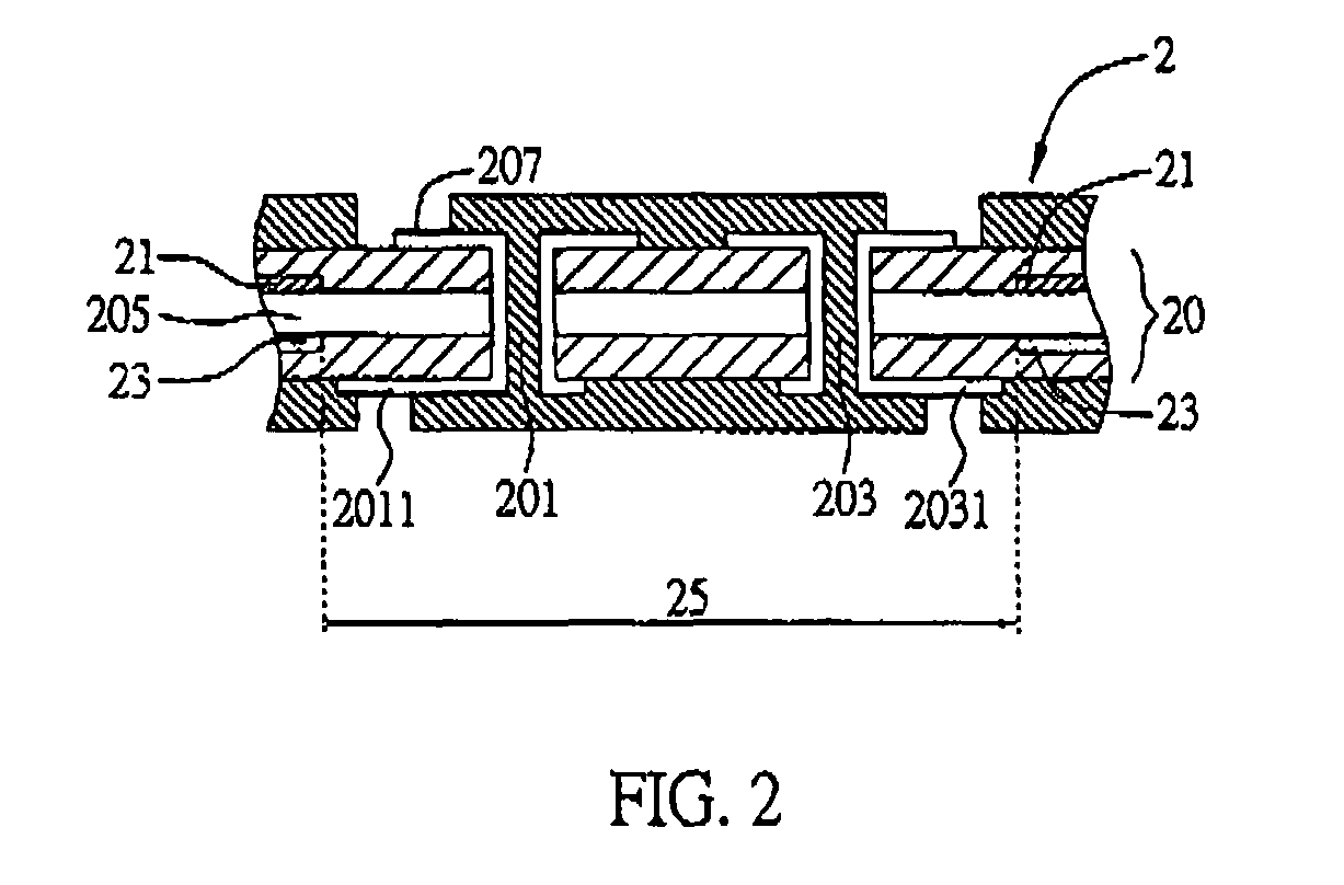
[0023]As shown in FIG. 2, a semiconductor package substrate 2 according to a first embodiment of the present invention comprises a substrate body 20 formed with a plurality of conductive through holes 201, 203 therein, wherein at least two adjacent conductive through holes 201, 203 are formed as a differential pair, each of which has a ball pad 2011, 2031 formed at an end thereof; and electrically integrated layers 21, 23 formed in the substrate body 20 and having an opening 25 corresponding to the conductive through holes 201, 203 formed as the differential pair and the ball pads 2011, 2031 thereof, wherein the opening 25 is sized larger enough to cover the conductive through holes 201, 203 formed as the differential pair and the ball pads 2011, 2031 thereof.

[0024]The substrate body 20 is a multi-layer printed circuit board (PCB) for use in a BGA semiconductor package. The substrate body 20 comprises at least one insulating core layer 205, and an inner circuit layer 207 formed on e...

second embodiment

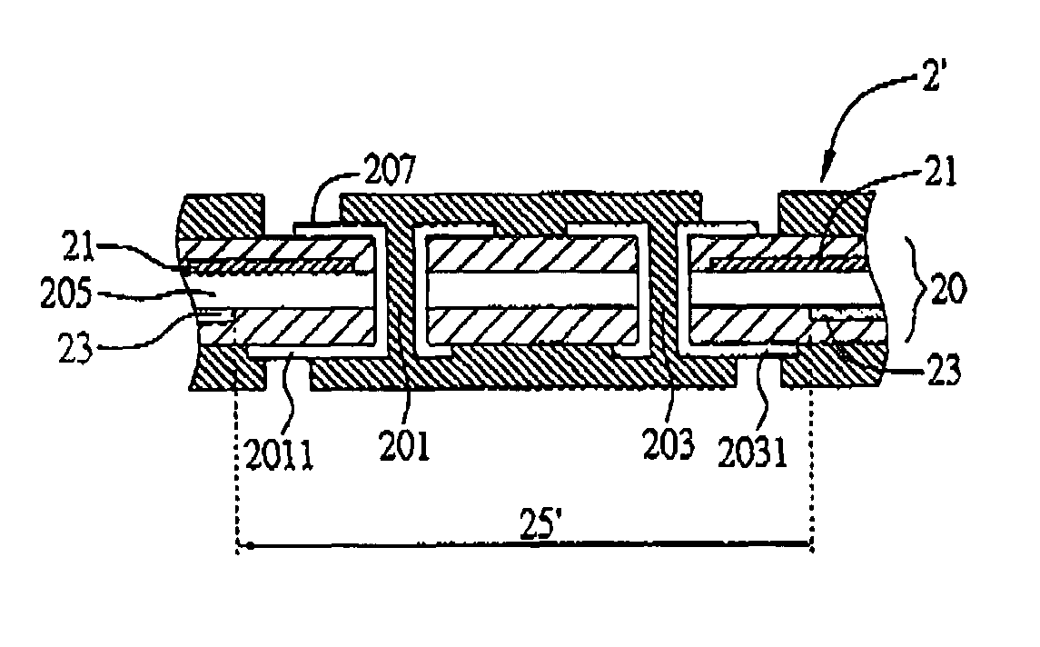
[0033]FIG. 4 is a cross-sectional view of a semiconductor package substrate 2′ according to a second embodiment of the present invention, wherein same or similar components are represented by same or similar reference numerals as compared with the first embodiment and detailed descriptions thereof may be omitted to allow the present invention to be more easily understood. The second embodiment primarily differs from the first embodiment in that, the opening penetrates only one of the electrically integrated layers, such as a power plane, which is relatively closer to the ball pads.

[0034]As shown in FIG. 4, the semiconductor package substrate 2′ comprises a substrate body 20 formed with a plurality of conductive through holes 201, 203 therein, wherein at least two adjacent conductive through holes 201, 203 are formed as a differential pair, each of which has a ball pad 2011, 2031 formed at an end thereof; electrically integrated layers 21, 23, such as a ground plane and a power plane...


PUM


Abstract

A semiconductor package substrate is provided, which includes a substrate body having a plurality of conductive through holes formed therein, wherein at least two adjacent conductive through holes are formed as a differential pair, each of which has a ball pad formed at an end thereof; and at least one electrically integrated layer formed in the substrate body, and having an opening corresponding to the two adjacent conductive through holes formed as the differential pair and the ball pads thereof. Thus, the spacing between the conductive through holes and the electrically integrated layer and the spacing between the ball pads can be enlarged by the opening, so as to balance the impedance match.

Description

FIELD OF THE INVENTION[0001]The present invention relates to semiconductor package substrates, and more particularly, to a semiconductor package substrate for balancing impedance match.BACKGROUND OF THE INVENTION[0002]For a semiconductor package substrate used in an electronic device, there have typically formed a plurality of through holes, such as plated through holes (PTHs), vias and blind holes, through the substrate in order to shorten a transmission path for chip signals. Further, at least a power plane and a ground plane are provided between multiple stacked layers of the substrate to enhance the electrical performance of a semiconductor package with the substrate. Accordingly, current may flow from the power plane of the substrate to a chip mounted on the substrate and then flow to the ground plane of the substrate via the plated through holes (having metal layers plated on walls of the through holes), thereby improving the electrical quality of the chip.[0003]When the chip ...

Claims


Application Information

Patent Timeline
Patent Type & Authority Patents(United States)
IPC IPC(8): H01L23/04
CPCH05K1/0251H05K1/114H01L23/49827H01L23/64H01L2223/6638H01L2924/3011H05K1/0245H05K3/429H05K2201/09236H01L2924/0002H05K2201/09636H05K2201/09718H01L2924/00
Inventor HSIEH, TSUNG-TIENCHIANG, WEN-JUNGWANG, YU-POHSIAO, CHENG-HSUYANG, SEN-YEN
Owner SILICONWARE PRECISION IND CO LTD
Why Eureka
Try Eureka