

Chemical mechanical polishing compositions for copper and associated materials and method of using same
a technology of mechanical polishing composition and copper, which is applied in the direction of polishing composition, other chemical processes, aqueous dispersions, etc., can solve the problems of poor planarization efficiency, oxide erosion, and micro-scratches of abrasive materials in slurries
- Summary
- Abstract
- Description
- Claims
- Application Information
AI Technical Summary
Benefits of technology
Problems solved by technology
Method used
Image

Examples
example 1
[0087]In one experiment 0.1% hydroxypropylcellulose with 1,000,000 MW was combined with:[0088]4% glycine;[0089]0.8% amino-tetrazole;[0090]5% hydrogen peroxide; and[0091]1% Nyacol DP6243 alumina coated silica composite abrasive.
[0092]The copper polish rate remained the same as without the addition of the rheology agent at approximately 4000 Å / min. However, tantalum (liner) polishing rate decreased from 40 Å / min to 30 Å / min, increasing selectivity from 100:1 to 133:1.
example 2
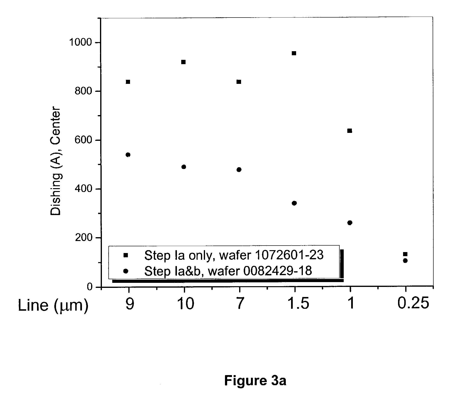
[0093]In a second experiment, the copper line dishing was compared between a one step copper polish using only the composition shown below under Step 1(a) and a two step (a&b) copper polish using the composition shown below under Step 1(a) and Step 1(b).
[0094]Step 1(a) Formulation
[0095]4% glycine;
[0096]0.8% amino-tetrazole;
[0097]5% hydrogen peroxide; and
[0098]1% alumina coated silica composite abrasive.
[0099]Step 1(b) Formulation
[0100]4% glycine;
[0101]0.8% amino-tetrazole;
[0103]1% alumina coated silica composite abrasive.
[0104]0.1% hydroxypropylcellulose with 1,000,000 MW;
[0105]FIGS. 3a through 3c compare dishing data of a Step 1(a&b) CMP process (circles) relative to a Step 1(a) only process (squares) for different line widths (isolated lines). A decrease in the concentration of the oxidizing agent prior to liner exposure reduces dishing effects by more than 500 Å (see 1.5 μm line width). The data is taken for different die on the wafer. FIGS. 3a, 3b an...
example 3
[0106]FIG. 4 shows electrical resistivity data for different overpolishing times for 100 μm lines. As the overpolishing time increases, so too does line dishing, which results in a decreasing of the cross section of the line. A decrease in the area of the cross section increases the electrical resistivity of the line. The relative increase in the line resistivity stays small in comparison to the line resistivity even for long overpolishing times. Thus a robust process is achieved by utilizing the described step 1a and 1b slurry to remove the Cu overburden and planarize the wafer surface.
PUM
| Property | Measurement | Unit |
|---|---|---|
| wt. % | aaaaa | aaaaa |
| weight | aaaaa | aaaaa |
| rheology | aaaaa | aaaaa |
Abstract
Description
Claims
Application Information